SNVS532D October 2007 – August 2020 LM5067
PRODUCTION DATA
- 1 Features
- 2 Applications
- 3 Description
- 4 Revision History
- 5 Device Comparison
- 6 Pin Configuration and Functions
- 7 Specifications
- 8 Detailed Description
-
9 Application and Implementation
- 9.1 Application Information
- 9.2
Typical Application
- 9.2.1 Design Requirements
- 9.2.2 Detailed Design Procedure
- 9.2.3 Application Curves
- 10Power Supply Recommendations
- 11Layout
- 12Device and Documentation Support
- 13Mechanical, Packaging, and Orderable Information
Package Options
Mechanical Data (Package|Pins)
Thermal pad, mechanical data (Package|Pins)
Orderable Information
9.2.2.10 Power Good Pin
During initial power up, the Power Good pin (PGD) is high until the operating voltage (VCC – VEE) increases above ≊2V. PGD then switches low, remaining low as the system voltage and the operating voltage increase. After Q1 is switched on, when the voltage at the OUT pin is within 1.23 V of the SENSE pin (Q1 VDS <1.23 V), PGD switches high indicating the output voltage is at, or nearly at, its final value. Any of the following situations will cause PGD to switch low within ≊10 µs:
- The VDS of Q1 increases above 2.5 V.
- The system input voltage decreases below the UVLO level.
- The system input voltage increase above the OVLO level.
- The TIMER pin increases to 4V due to a fault condition.
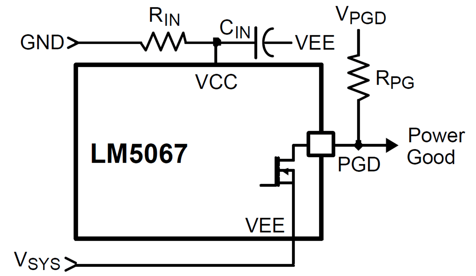
A pull-up resistor is required at PGD as shown in Figure 9-12. The pull-up voltage (VPGD) can be as high as 80 V above VEE, with transient capability to 100 V, and can be higher or lower than the system ground.
 Figure 9-12 Power Good Output
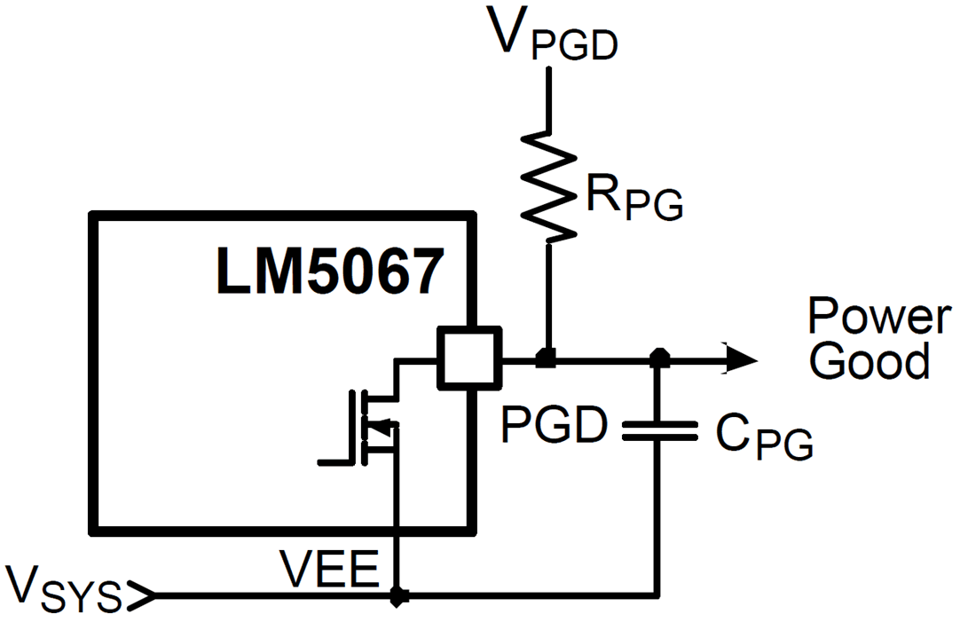
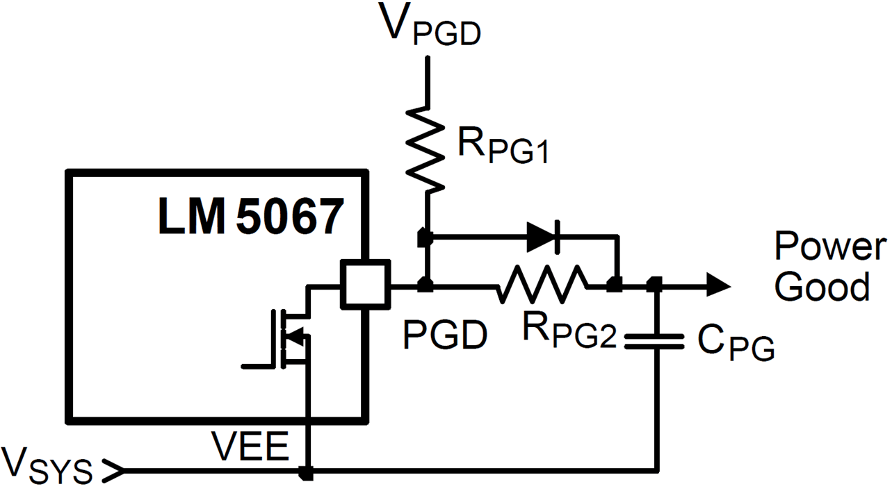
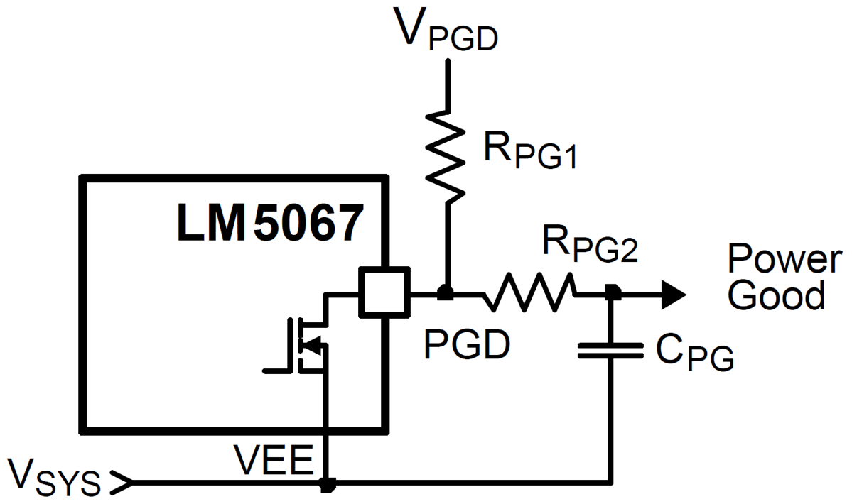
If a delay is required at PGD, suggested circuits are shown in the following figure. In Figure 9-13, capacitor CPG adds delay to the rising edge, but not to the falling edge. In Figure 9-14, the rising edge is delayed by RPG1 + RPG2 and CPG, while the falling edge is delayed a lesser amount by RPG2 and CPG. Adding a diode across RPG2. Figure 9-15 allows for equal delays at the two edges, or a short delay at the rising edge and a long delay at the falling edge.
 Figure 9-13 Adding Delay to the Power Good Output Pin - Delay Rising Edge Only
 Figure 9-15 Adding Delay to the Power Good Output Pin - Short Delay at Rising Edge and Long Delay at Falling Edge, or Equal Delays
 Figure 9-14 Adding Delay to the Power Good Output Pin - Long Delay at Rising Edge, Short Delay at Falling Edge