SNVS532D October 2007 – August 2020 LM5067
PRODUCTION DATA
- 1 Features
- 2 Applications
- 3 Description
- 4 Revision History
- 5 Device Comparison
- 6 Pin Configuration and Functions
- 7 Specifications
- 8 Detailed Description
-
9 Application and Implementation
- 9.1 Application Information
- 9.2
Typical Application
- 9.2.1 Design Requirements
- 9.2.2 Detailed Design Procedure
- 9.2.3 Application Curves
- 10Power Supply Recommendations
- 11Layout
- 12Device and Documentation Support
- 13Mechanical, Packaging, and Orderable Information
Package Options
Mechanical Data (Package|Pins)
Thermal pad, mechanical data (Package|Pins)
Orderable Information
8.3.2 Gate Control
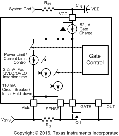
The external N-channel MOSFET is turned on when the GATE pin sources 52 µA to enhance the gate. During normal operation (t3 in Figure 8-2) Q1’s gate is held charged to approximately 13V above VEE, typically within 20 mV of the voltage at VCC. If the maximum VGS rating of Q1 is less than 13V, a lower voltage external zener diode must be added between the GATE and SENSE pins. The external zener diode must have a forward current rating of at least 110 mA.
When the system voltage is initially applied (before the operating voltage reaches the PORIT threshold), the GATE pin is held low by a 110 mA pull-down current. The pull-down current helps prevent an inadvertent turn-on of the MOSFET through its drain-gate capacitance as the applied system voltage increases.
During the insertion time (t1 in Figure 8-2) the GATE pin is held low by a 2.2 mA pull-down current. This maintains Q1 in the off-state until the end of t1, regardless of the voltage at VCC and UVLO.
Following the insertion time, during t2 in Figure 8-2, the gate voltage of Q1 is modulated to keep the current or Q1’s power dissipation level from exceeding the programmed levels. Current limiting and power limiting are considered fault conditions, during which the voltage on the TIMER pin capacitor increases. If the current and power limiting cease before the TIMER pin reaches 4 V the TIMER pin capacitor is discharged, and the circuit enters normal operation. See Fault Timer and Restart for details on the fault timer.
If the system input voltage falls below the UVLO threshold, or rises above the OVLO threshold, the GATE pin is pulled low by the 2.2 mA pull-down current to switch off Q1.
 Figure 8-3 Gate Control