SNVS268B May 2004 – December 2014 LM5102
PRODUCTION DATA.
- 1 Features
- 2 Applications
- 3 Description
- 4 Revision History
- 5 Pin Configuration and Functions
- 6 Specifications
- 7 Detailed Description
- 8 Application and Implementation
- 9 Power Supply Recommendations
- 10Layout
- 11Device and Documentation Support
- 12Mechanical, Packaging, and Orderable Information
Package Options
Mechanical Data (Package|Pins)
Thermal pad, mechanical data (Package|Pins)
- DPR|10
Orderable Information
1 Features
- Drives Both a High-Side and Low-Side N-Channel MOSFET
- Independently Programmable High and Low Side Rising Edge Delay
- Bootstrap Supply Voltage Range up to 118 V dc
- Fast Turn-Off Propagation Delay (25 ns Typical)
- Drives 1000-pF Loads with 15-ns Rise and Fall Times
- Supply Rail Undervoltage Lockout
- Low Power Consumption
- Timer Can Be Terminated Midway Through Sequence
2 Applications
- Current Fed Push-Pull Power Converters
- Half and Full Bridge Power Converters
- Synchronous Buck Converters
- Two Switch Forward Power Converters
- Forward with Active Clamp Converters
3 Description
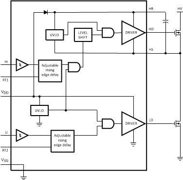
The LM5102 high-voltage gate driver is designed to drive both the high side and the low side N-Channel MOSFETs in a synchronous buck or a half bridge configuration. The floating high-side driver is capable of working with supply voltages up to 100 V. The outputs are independently controlled. The rising edge of each output can be independently delayed with a programming resistor. An integrated high voltage diode is provided to charge the high side gate drive bootstrap capacitor. A robust level shifter operates at high speed while consuming low power and providing clean level transitions from control logic to the high side gate driver. Undervoltage lockout is provided on both the low side and the high side power rails. This device is available in the standard VSSOP 10 pin and the WSON 10 pin packages.
Device Information(1)
| PART NUMBER | PACKAGE | BODY SIZE (NOM) |
|---|---|---|
| LM5102 | VSSOP (10) | 3.00 mm × 3.00 mm |
| WSON (10) | 4.00 mm × 4.00 mm |
- For all available packages, see the orderable addendum at the end of the data sheet.
Simplified Block Diagram