SNVS268B May 2004 – December 2014 LM5102
PRODUCTION DATA.
- 1 Features
- 2 Applications
- 3 Description
- 4 Revision History
- 5 Pin Configuration and Functions
- 6 Specifications
- 7 Detailed Description
- 8 Application and Implementation
- 9 Power Supply Recommendations
- 10Layout
- 11Device and Documentation Support
- 12Mechanical, Packaging, and Orderable Information
Package Options
Mechanical Data (Package|Pins)
Thermal pad, mechanical data (Package|Pins)
- DPR|10
Orderable Information
6 Specifications
6.1 Absolute Maximum Ratings(1)(2)
| MIN | MAX | UNIT | |
|---|---|---|---|
| VDD to VSS | –0.3 | 18 | V |
| VHB to VHS | –0.3 | 18 | V |
| LI or HI Inputs to VSS | –0.3 | VDD + 0.3 | V |
| LO Output | –0.3 | VDD + 0.3 | V |
| HO Output | VHS – 0.3 | VHB + 0.3 | V |
| VHS to VSS | –1 | 100 | V |
| VHB to VSS | 118 | V | |
| RT1 and RT2 to VSS | –0.3 | 5 | V |
| Junction Temperature | 150 | °C | |
| Storage Temperature Range | –55 | 150 | °C |
(1) Stresses beyond those listed under Absolute Maximum Ratings may cause permanent damage to the device. These are stress ratings only, which do not imply functional operation of the device at these or any other conditions beyond those indicated under Recommended Operating Conditions. Exposure to absolute-maximum-rated conditions for extended periods may affect device reliability.
(2) If Military/Aerospace specified devices are required, please contact the Texas Instruments Sales Office/Distributors for availability and specifications.
6.2 ESD Ratings
| VALUE | UNIT | |||
|---|---|---|---|---|
| V(ESD) | Electrostatic discharge | Human-body model (HBM), per ANSI/ESDA/JEDEC JS-001(1) | ±2000 | V |
(1) JEDEC document JEP155 states that 500-V HBM allows safe manufacturing with a standard ESD control process.
6.3 Recommended Operating Conditions
| MIN | MAX | UNIT | |
|---|---|---|---|
| VDD | 9 | 14 | V |
| HS | –1 | 100 | V |
| HB | VHS + 8 | VHS + 14 | V |
| HS Slew Rate | < 50 | V/ns | |
| Junction Temperature | –40 | 125 | °C |
6.4 Thermal Information
| THERMAL METRIC(1) | LM5102 | UNIT | ||
|---|---|---|---|---|
| DGS | DPR(2) | |||
| 10 PINS | 10 PINS | |||
| RθJA | Junction-to-ambient thermal resistance | 165.3 | 37.9 | °C/W |
| RθJC(top) | Junction-to-case (top) thermal resistance | 58.9 | 38.1 | |
| RθJB | Junction-to-board thermal resistance | 54.4 | 14.9 | |
| ψJT | Junction-to-top characterization parameter | 6.2 | 0.4 | |
| ψJB | Junction-to-board characterization parameter | 83.6 | 15.2 | |
| RθJC(bot) | Junction-to-case (bottom) thermal resistance | N/A | 4.4 | |
(1) For more information about traditional and new thermal metrics, see the IC Package Thermal Metrics application report (SPRA953).
(2) 4 layer board with Cu finished thickness 1.5 oz, 1 oz, 1 oz, 1.5 oz. Maximum die size used. 5x body length of Cu trace on PCB top. 50 x 50 mm ground and power planes embedded in PCB. See Application Note AN-1187 Leadless Leadframe Package (LLP) (SNOA401).
6.5 Electrical Characteristics
Specifications in standard typeface are for TJ = +25°C. Unless otherwise specified, VDD = VHB = 12 V, VSS = VHS = 0V, RT1 = RT2 = 100 kΩ. No load on LO or HO.| PARAMETER | TEST CONDITIONS | MIN(1) | TYP | MAX(1) | UNIT | |
|---|---|---|---|---|---|---|
| SUPPLY CURRENTS | ||||||
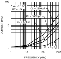
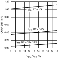
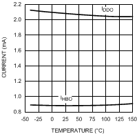
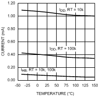
| IDD | VDD Quiescent Current | LI = HI = 0 V | 0.4 | mA | ||
| LI = HI = 0 V, –40°C to +125°C | 0.6 | |||||
| IDDO | VDD Operating Current | f = 500 kHz | 1.5 | mA | ||
| f = 500 kHz, –40°C to +125°C | 3 | |||||
| IHB | Total HB Quiescent Current | LI = HI = 0 V | 0.06 | mA | ||
| LI = HI = 0 V, –40°C to +125°C | 0.2 | |||||
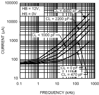
| IHBO | Total HB Operating Current | f = 500 kHz | 1.3 | mA | ||
| f = 500 kHz, –40°C to +125°C | 3 | |||||
| IHBS | HB to VSS Current, Quiescent | VHS = VHB = 100 V | 0.05 | µA | ||
| VHS = VHB = 100 V, –40°C to +125°C | 10 | |||||
| IHBSO | HB to VSS Current, Operating | f = 500 kHz | 0.08 | mA | ||
| INPUT PINS | ||||||
| VIL | Low Level Input Voltage Threshold | 1.8 | V | |||
| –40°C to +125°C | 0.8 | |||||
| VIH | High Level Input Voltage Threshold | 1.8 | V | |||
| –40°C to +125°C | 2.2 | |||||
| RI | Input Pulldown Resistance | 200 | kΩ | |||
| –40°C to +125°C | 100 | 500 | ||||
| TIME DELAY CONTROLS | ||||||
| VRT | Nominal Voltage at RT1, RT2 | 3 | V | |||
| –40°C to +125°C | 2.7 | 3.3 | ||||
| IRT | RT Pin Current Limit | RT1 = RT2 = 0 V | 1.5 | mA | ||
| RT1 = RT2 = 0 V, –40°C to +125°C | 0.75 | 2.25 | ||||
| Vth | Timer Termination Threshold | 1.8 | V | |||
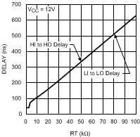
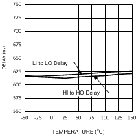
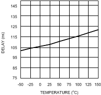
| TDL1, TDH1 | Rising edge turn-on delay, RT = 10 kΩ | 105 | ns | |||
| –40°C to +125°C | 75 | 150 | ||||
| TDL2, TDH2 | Rising edge turn-on delay, RT = 100 kΩ | 630 | ns | |||
| –40°C to +125°C | 530 | 750 | ||||
| UNDER VOLTAGE PROTECTION | ||||||
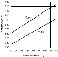
| VDDR | VDD Rising Threshold | 6.9 | V | |||
| –40°C to +125°C | 6.0 | 7.4 | ||||
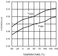
| VDDH | VDD Threshold Hysteresis | 0.5 | V | |||
| VHBR | HB Rising Threshold | 6.6 | V | |||
| –40°C to +125°C | 5.7 | 7.1 | ||||
| VHBH | HB Threshold Hysteresis | 0.4 | V | |||
| BOOTSTRAP DIODE | ||||||
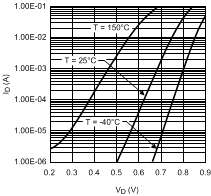
| VDL | Low-Current Forward Voltage | IVDD-HB = 100 µA | 0.60 | V | ||
| IVDD-HB = 100 µA, –40°C to +125°C | 0.9 | |||||
| VDH | High-Current Forward Voltage | IVDD-HB = 100 mA | 0.85 | V | ||
| IVDD-HB = 100 mA, –40°C to +125°C | 1.1 | |||||
| RD | Dynamic Resistance | IVDD-HB = 100 mA | 0.8 | Ω | ||
| IVDD-HB = 100 mA, –40°C to +125°C | 1.5 | |||||
| LO GATE DRIVER | ||||||
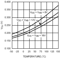
| VOLL | Low-Level Output Voltage | ILO = 100 mA | 0.25 | V | ||
| ILO = 100 mA, –40°C to +125°C | 0.4 | |||||
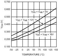
| VOHL | High-Level Output Voltage | ILO = –100 mA, VOHL = VDD – VLO | 0.35 | V | ||
| ILO = –100 mA, VOHL = VDD – VLO, –40°C to +125°C | 0.55 | |||||
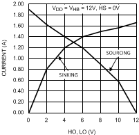
| IOHL | Peak Pullup Current | VLO = 0 V | 1.6 | A | ||
| IOLL | Peak Pulldown Current | VLO = 12 V | 1.8 | A | ||
| HO GATE DRIVER | ||||||
| VOLH | Low-Level Output Voltage | IHO = 100 mA | 0.25 | V | ||
| IHO = 100 mA, –40°C to +125°C | 0.4 | |||||
| VOHH | High-Level Output Voltage | IHO = –100 mA, VOHH = VHB – VHO | 0.35 | V | ||
| IHO = –100 mA, VOHH = VHB – VHO, –40°C to +125°C | 0.55 | |||||
| IOHH | Peak Pullup Current | VHO = 0 V | 1.6 | A | ||
| IOLH | Peak Pulldown Current | VHO = 12 V | 1.8 | A | ||
6.6 Switching Characteristics
Specifications in standard typeface are for TJ = +25°C. Unless otherwise specified, VDD = VHB = 12 V, VSS = VHS = 0 V, No Load on LO or HO.| PARAMETER | TEST CONDITIONS | MIN(1) | TYP | MAX(1) | UNIT | |
|---|---|---|---|---|---|---|
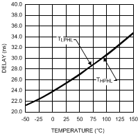
| tLPHL | Lower Turn-Off Propagation Delay LM5102 (LI Falling to LO Falling) |
27 | ns | |||
| –40°C to +125°C | 56 | |||||
| tHPHL | Upper Turn-Off Propagation Delay LM5102 (HI Falling to HO Falling) |
27 | ns | |||
| –40°C to +125°C | 56 | |||||
| tRC, tFC | Either Output Rise/Fall Time | CL = 1000 pF | 15 | ns | ||
| tR, tF | Either Output Rise/Fall Time (3 V to 9 V) | CL = 0.1 µF | 0.6 | µs | ||
| tBS | Bootstrap Diode Turn-Off Time | IF = 20 mA, IR = 200 mA | 50 | ns | ||
(1) MIN and MAX limits are 100% production tested at 25°C. Limits over the operating temperature range are specified through correlation using Statistical Quality Control (SQC) methods. Limits are used to calculate TI’s Average Outgoing Quality Level (AOQL).
6.7 Typical Characteristics