SNVS268B May 2004 – December 2014 LM5102
PRODUCTION DATA.
- 1 Features
- 2 Applications
- 3 Description
- 4 Revision History
- 5 Pin Configuration and Functions
- 6 Specifications
- 7 Detailed Description
- 8 Application and Implementation
- 9 Power Supply Recommendations
- 10Layout
- 11Device and Documentation Support
- 12Mechanical, Packaging, and Orderable Information
Package Options
Mechanical Data (Package|Pins)
Thermal pad, mechanical data (Package|Pins)
- DPR|10
Orderable Information
7 Detailed Description
7.1 Overview
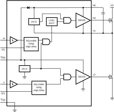
The LM5102 device offers a unique flexibility with independently programmable delay of the rising edge for both high and low side driver outputs independently. The delays are set with resistors at the RT1 and RT2 pins, and can be adjusted from 100 ns to 600 ns. This feature reduces component count, board space and cost compared to discrete solutions for adjusting driver dead time. The wide delay programming range provides the flexibility to optimize drive signal timing for a wide range of MOSFETs and applications.
The RT pins are biased at 3 V and current limited to 1 mA maximum programming current. The time delay generator will accommodate resistor values from 5 k to 100 k with turn-on delay times that are proportional to the RT resistance. In addition, each RT pin is monitored by a comparator that will bypass the turn-on delay if the RT pin is pulled below the timer elimination threshold (1.8 V typical). Grounding the RT pins programs the LM5102 to drive both outputs with minimum turn-on delay.
7.2 Functional Block Diagram
7.3 Feature Description
7.3.1 Startup and UVLO
Both top and bottom drivers include undervoltage lockout (UVLO) protection circuitry which monitors the supply voltage (VDD) and bootstrap capacitor voltage (VHB – VHS) independently. The UVLO circuit inhibits each driver until sufficient supply voltage is available to turn-on the external MOSFETs, and the built-in hysteresis prevents chattering during supply voltage transitions. When the supply voltage is applied to VDD pin of LM5102, the top and bottom gates are held low until VDD exceeds UVLO threshold, typically about 6.9 V. Any UVLO condition on the bootstrap capacitor will disable only the high side output (HO).
7.4 Device Functional Modes
| LI Pin | LO Pin | HI Pin | HO Pin |
|---|---|---|---|
| L | L | L | L |
| H | H | H | H |