SNVS268B May 2004 – December 2014 LM5102
PRODUCTION DATA.
- 1 Features
- 2 Applications
- 3 Description
- 4 Revision History
- 5 Pin Configuration and Functions
- 6 Specifications
- 7 Detailed Description
- 8 Application and Implementation
- 9 Power Supply Recommendations
- 10Layout
- 11Device and Documentation Support
- 12Mechanical, Packaging, and Orderable Information
Package Options
Mechanical Data (Package|Pins)
Thermal pad, mechanical data (Package|Pins)
- DPR|10
Orderable Information
10 Layout
10.1 Layout Guidelines
The optimum performance of high and low side gate drivers cannot be achieved without taking due considerations during circuit board layout. Following points are emphasized.
- A low ESR/ESL capacitor must be connected close to the IC, and between VDD and VSS pins and between HB and HS pins to support high peak currents being drawn from VDD during turn-on of the external MOSFET.
- To prevent large voltage transients at the drain of the top MOSFET, a low ESR electrolytic capacitor must be connected between MOSFET drain and ground (VSS).
- In order to avoid large negative transients on the switch node (HS) pin, the parasitic inductances in the source of top MOSFET and in the drain of the bottom MOSFET (synchronous rectifier) must be minimized.
- Grounding considerations:
- The first priority in designing grounding connections is to confine the high peak currents from charging and discharging the MOSFET gate in a minimal physical area. This will decrease the loop inductance and minimize noise issues on the gate terminal of the MOSFET. The MOSFETs should be placed as close as possible to the gate driver.
- The second high current path includes the bootstrap capacitor, the bootstrap diode, the local ground referenced bypass capacitor and low side MOSFET body diode. The bootstrap capacitor is recharged on the cycle-by-cycle basis through the bootstrap diode from the ground referenced VDD bypass capacitor. The recharging occurs in a short time interval and involves high peak current. Minimizing this loop length and area on the circuit board is important to ensure reliable operation.
- The resistors on the RT1 and RT2 timer pins must be placed very close to the IC and seperated from high current paths to avoid noise coupling to the time delay generator which could disrupt timer operation.
10.2 Layout Example
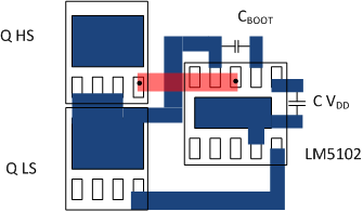 Figure 22. LM5102 Component Placement