SNVS268B May 2004 – December 2014 LM5102
PRODUCTION DATA.
- 1 Features
- 2 Applications
- 3 Description
- 4 Revision History
- 5 Pin Configuration and Functions
- 6 Specifications
- 7 Detailed Description
- 8 Application and Implementation
- 9 Power Supply Recommendations
- 10Layout
- 11Device and Documentation Support
- 12Mechanical, Packaging, and Orderable Information
Package Options
Mechanical Data (Package|Pins)
Thermal pad, mechanical data (Package|Pins)
- DPR|10
Orderable Information
5 Pin Configuration and Functions
10 Pin
VSSOP (DGS), WSON (DPR)
Top View
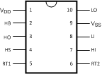
Pin Functions
| PIN | TYPE(2) | DESCRIPTION | APPLICATION INFORMATION | |
|---|---|---|---|---|
| NAME | WSON(1), VSSOP |
|||
| HB | 2 | P | High-side gate driver bootstrap rail | Connect the positive terminal of bootstrap capacitor to the HB pin and connect negative terminal of bootstrap capacitor to HS. The Bootstrap capacitor should be placed as close to IC as possible. |
| HI | 7 | I | High-side driver control input | TTL compatible thresholds. Unused inputs should be tied to ground and not left open. |
| HO | 3 | O | High-side gate driver output | Connect to gate of high-side MOSFET with short low-inductance path. |
| HS | 4 | P | High-side MOSFET source connection | Connect bootstrap capacitor negative terminal and source of high side MOSFET. |
| LI | 8 | I | Low-side driver control input | TTL compatible thresholds. Unused inputs should be tied to ground and not left open. |
| LO | 10 | O | Low-side gate driver output | Connect to the gate of the low side MOSFET with a short low inductance path. |
| RT1 | 5 | A | High-side output edge delay programming | Resistor from RT1 to ground programs the leading edge delay of the high side gate driver. The resistor should be placed close to the IC to minimize noise coupling from adjacent traces. |
| RT2 | 6 | A | Low-side output edge delay programming | Resistor from RT2 to ground programs the leading edge delay of the low side gate driver. The resistor should be placed close to the IC to minimize noise coupling from adjacent traces. |
| VDD | 1 | P | Positive gate drive supply | Locally decouple to VSS using low ESR/ESL capacitor, located as close to IC as possible. |
| VSS | 9 | G | Ground return | All signals are referenced to this ground. |
(1) For the WSON package, it is recommended that the exposed pad on the bottom of the LM5100 and LM5101 be soldered to ground plane on the PC board, and the ground plane should extend out from beneath the IC to help dissipate the heat.
(2) P = Power, G = Ground, I = Input, O = Output, A = Analog