SNVS269D January 2004 – December 2014 LM5104
PRODUCTION DATA.
- 1 Features
- 2 Applications
- 3 Description
- 4 Revision History
- 5 Pin Configuration and Functions
- 6 Specifications
- 7 Detailed Description
- 8 Application and Implementation
- 9 Power Supply Recommendations
- 10Layout
- 11Device and Documentation Support
- 12Mechanical, Packaging, and Orderable Information
Package Options
Mechanical Data (Package|Pins)
Thermal pad, mechanical data (Package|Pins)
- DPR|10
Orderable Information
1 Features
- Drives Both a High-Side and Low-Side N-Channel MOSFET
- Adaptive Rising and Falling Edges With Programmable Additional Delay
- Single Input Control
- Bootstrap Supply Voltage Range up to 118-V DC
- Fast Turnoff Propagation Delay (25 ns Typical)
- Drives 1000-pF Loads With 15-ns Rise and Fall Times
- Supply Rail Undervoltage Lockout
- SOIC and WSON-10 4-mm × 4-mm Package
2 Applications
- Current Fed Push-Pull Power Converters
- High Voltage Buck Regulators
- Active Clamp Forward Power Converters
- Half-Bridge and Full-Bridge Converters
3 Description
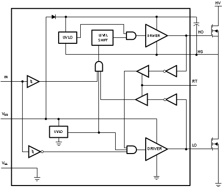
The LM5104 High-Voltage Gate Driver is designed to drive both the high-side and the low-side N-channel MOSFETs in a synchronous buck configuration. The floating high-side driver can work with supply voltages up to 100 V. The high-side and low-side gate drivers are controlled from a single input. Each change in state is controlled in an adaptive manner to prevent shoot-through issues. In addition to the adaptive transition timing, an additional delay time can be added, proportional to an external setting resistor. An integrated high-voltage diode is provided to charge high-side gate drive bootstrap capacitor. A robust level shifter operates at high speed while consuming low power and providing clean level transitions from the control logic to the high-side gate driver. Undervoltage lockout is provided on both the low-side and the high-side power rails. This device is available in the standard SOIC and the WSON packages.
Device Information(1)
| PART NUMBER | PACKAGE | BODY SIZE (NOM) |
|---|---|---|
| LM5104 | SOIC (8) | 4.90 mm × 3.91 mm |
| WSON (10) | 4.00 mm × 4.00 mm |
- For all available packages, see the orderable addendum at the end of the datasheet.
Simplified Block Diagram