SNVS269D January 2004 – December 2014 LM5104
PRODUCTION DATA.
- 1 Features
- 2 Applications
- 3 Description
- 4 Revision History
- 5 Pin Configuration and Functions
- 6 Specifications
- 7 Detailed Description
- 8 Application and Implementation
- 9 Power Supply Recommendations
- 10Layout
- 11Device and Documentation Support
- 12Mechanical, Packaging, and Orderable Information
Package Options
Mechanical Data (Package|Pins)
Thermal pad, mechanical data (Package|Pins)
- DPR|10
Orderable Information
9 Power Supply Recommendations
9.1 Power Dissipation Considerations
The total IC power dissipation is the sum of the gate driver losses and the bootstrap diode losses. The gate driver losses are related to the switching frequency (f), output load capacitance on LO and HO (CL), and supply voltage (VDD) and can be roughly calculated as:
There are some additional losses in the gate drivers due to the internal CMOS stages used to buffer the LO and HO outputs. The plot in Figure 18 shows the measured gate driver power dissipation versus frequency and load capacitance. At higher frequencies and load capacitance values, the power dissipation is dominated by the power losses driving the output loads and agrees well with Equation 12. This plot can be used to approximate the power losses due to the gate drivers.
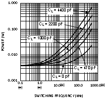 Figure 18. Gate Driver Power Dissipation (LO + HO)
VCC = 12V, Neglecting Diode Losses
The bootstrap diode power loss is the sum of the forward bias power loss that occurs while charging the bootstrap capacitor and the reverse bias power loss that occurs during reverse recovery. Since each of these events happens once per cycle, the diode power loss is proportional to frequency. Larger capacitive loads require more current to recharge the bootstrap capacitor resulting in more losses. Higher input voltages (VIN) to the half bridge result in higher reverse recovery losses. The following plot was generated based on calculations and lab measurements of the diode recovery time and current under several operating conditions. This can be useful for approximating the diode power dissipation.
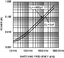 Figure 19. Diode Power Dissipation VIN = 80V
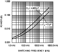 Figure 20. Diode Power Dissipation VIN = 40V
The total IC power dissipation can be estimated from the above plots by summing the gate drive losses with the bootstrap diode losses for the intended application. Because the diode losses can be significant, an external diode placed in parallel with the internal bootstrap diode (refer to Figure 15) can be helpful in removing power from the IC. For this to be effective, the external diode must be placed close to the IC to minimize series inductance and have a significantly lower forward voltage drop than the internal diode.