SNVS269D January 2004 – December 2014 LM5104
PRODUCTION DATA.
- 1 Features
- 2 Applications
- 3 Description
- 4 Revision History
- 5 Pin Configuration and Functions
- 6 Specifications
- 7 Detailed Description
- 8 Application and Implementation
- 9 Power Supply Recommendations
- 10Layout
- 11Device and Documentation Support
- 12Mechanical, Packaging, and Orderable Information
Package Options
Mechanical Data (Package|Pins)
Thermal pad, mechanical data (Package|Pins)
- DPR|10
Orderable Information
7 Detailed Description
7.1 Overview
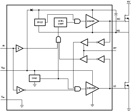
The LM5104 High Voltage gate driver is designed to drive both the high side and the low side N-Channel MOSFETs in a synchronous buck configuration. The floating high-side driver is capable of working with supply voltages up to 100 V. The high side and low side gate drivers are controlled from a single input. Each change in state is controlled in an adaptive manner to prevent shoot-through issues. In addition to the adaptive transition timing, an additional delay time can be added, proportional to an external setting resistor. An integrated high voltage diode is provided to charge high side gate drive bootstrap capacitor. A robust level shifter operates at high speed while consuming low power and providing clean level transitions from the control logic to the high side gate driver. Under-voltage lockout is provided on both the low side and the high side power rails.
7.2 Functional Block Diagram
7.3 Feature Description
7.3.1 Adaptive Shoot-Through Protection
LM5104 is a high voltage, high speed dual output driver designed to drive top and bottom MOSFET’s connected in synchronous buck or half-bridge configuration, from one externally provided PWM signal. LM5104 features adaptive delay to prevent shoot-through current through top and bottom MOSFETs during switching transitions. Referring to the timing diagram Figure 16, the rising edge of the PWM input (IN) turns off the bottom MOSFET (LO) after a short propagation delay (tP). An adaptive circuit in the LM5104 monitors the bottom gate voltage (LO) and triggers a programmable delay generator when the LO pin falls below an internally set threshold (≈ Vdd/2). The gate drive of the upper MOSFET (HO) is disabled until the deadtime expires. The upper gate is enabled after the TIMER delay (tP+TRT), and the upper MOSFET turns-on. The additional delay of the timer prevents lower and upper MOSFETs from conducting simultaneously, thereby preventing shoot-through.
A falling transition on the PWM signal (IN) initiates the turn-off of the upper MOSFET and turn-on of the lower MOSFET. A short propagation delay (tP) is encountered before the upper gate voltage begins to fall. Again, the adaptive shoot-through circuitry and the programmable deadtime TIMER delays the lower gate turn-on time. The upper MOSFET gate voltage is monitored and the deadtime delay generator is triggered when the upper MOSFET gate voltage with respect to ground drops below an internally set threshold (≈ Vdd/2). The lower gate drive is momentarily disabled by the timer and turns on the lower MOSFET after the deadtime delay expires (tP+TRT).
The RT pin is biased at 3V and current limited to 1mA. It is designed to accommodate a resistor between 5K and 100K, resulting in an effective dead-time proportional to RT and ranging from 90ns to 200ns. RT values below 5K will saturate the timer and are not recommended.
7.3.2 Start-up and UVLO
Both top and bottom drivers include undervoltage lockout (UVLO) protection circuitry which monitors the supply voltage (VDD) and bootstrap capacitor voltage (VHB – VHS) independently. The UVLO circuit inhibits each driver until sufficient supply voltage is available to turn-on the external MOSFETs, and the built-in hysteresis prevents chattering during supply voltage transitions. When the supply voltage is applied to VDD pin of LM5104, the top and bottom gates are held low until VDD exceeds UVLO threshold, typically about 6.9 V. Any UVLO condition on the bootstrap capacitor will disable only the high-side output (HO).
7.4 Device Functional Modes
| IN Pin | LO Pin | HO Pin |
|---|---|---|
| L | H | L |
| H | L | H |