SNVS499I February 2007 – November 2023 LM5116
PRODUCTION DATA
- 1
- 1 Features
- 2 Applications
- 3 Description
- 4 Pin Configuration and Functions
- 5 Specifications
- 6 Detailed Description
-
7 Application and Implementation
- 7.1 Application Information
- 7.2
Typical Application
- 7.2.1 Design Requirements
- 7.2.2
Detailed Design Procedure
- 7.2.2.1 Custom Design with WEBENCH® Tools
- 7.2.2.2 Timing Resistor
- 7.2.2.3 Output Inductor
- 7.2.2.4 Current Sense Resistor
- 7.2.2.5 Ramp Capacitor
- 7.2.2.6 Output Capacitors
- 7.2.2.7 Input Capacitors
- 7.2.2.8 VCC Capacitor
- 7.2.2.9 Bootstrap Capacitor
- 7.2.2.10 Soft Start Capacitor
- 7.2.2.11 Output Voltage Divider
- 7.2.2.12 UVLO Divider
- 7.2.2.13 MOSFETs
- 7.2.2.14 MOSFET Snubber
- 7.2.2.15 Error Amplifier Compensation
- 7.2.2.16 Comprehensive Equations
- 7.2.3 Application Curves
- 7.3 Power Supply Recommendations
- 7.4 Layout
- 8 Device and Documentation Support
- 9 Revision History
- 10Mechanical, Packaging, and Orderable Information
Package Options
Mechanical Data (Package|Pins)
- PWP|20
Thermal pad, mechanical data (Package|Pins)
- PWP|20
Orderable Information
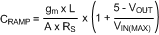
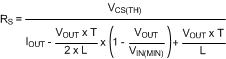
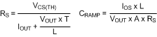
7.2.2.16.1 Current Sense Resistor and Ramp Capacitor
T = 1 / fSW, gm = 5 µA/V, A = 10 V/V. IOUT is the maximum output current at current limit.
General Method for VOUT < 5 V:
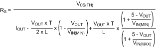
General Method for 5 V < VOUT < 7.5 V:
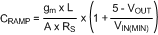
Best Performance Method:
This minimizes the current limit deviation due to changes in line voltage, while maintaining near optimal slope compensation.
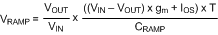
Calculate optimal slope current, IOS = (VOUT / 3) ✕ 10 µA/V. For example, at VOUT = 7.5 V, IOS = 25 µA.
Calculate VRAMP at the nominal input voltage.
For VOUT > 7.5 V, install a resistor from the RAMP pin to VCC.
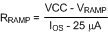
 Figure 7-6 RRAMP to VCC for VOUT > 7.5 V
For VOUT < 7.5 V, a negative VCC is required. This can be made with a simple charge pump from the LO gate output. Install a resistor from the RAMP pin to the negative VCC.
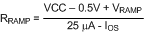
 Figure 7-7 RRAMP to -VCC for VOUT < 7.5 V
If a large variation is expected in VCC, say for VIN < 11 V, a Zener regulator can be added to supply a constant voltage for RRAMP.