SNVS499I February 2007 – November 2023 LM5116
PRODUCTION DATA
- 1
- 1 Features
- 2 Applications
- 3 Description
- 4 Pin Configuration and Functions
- 5 Specifications
- 6 Detailed Description
-
7 Application and Implementation
- 7.1 Application Information
- 7.2
Typical Application
- 7.2.1 Design Requirements
- 7.2.2
Detailed Design Procedure
- 7.2.2.1 Custom Design with WEBENCH® Tools
- 7.2.2.2 Timing Resistor
- 7.2.2.3 Output Inductor
- 7.2.2.4 Current Sense Resistor
- 7.2.2.5 Ramp Capacitor
- 7.2.2.6 Output Capacitors
- 7.2.2.7 Input Capacitors
- 7.2.2.8 VCC Capacitor
- 7.2.2.9 Bootstrap Capacitor
- 7.2.2.10 Soft Start Capacitor
- 7.2.2.11 Output Voltage Divider
- 7.2.2.12 UVLO Divider
- 7.2.2.13 MOSFETs
- 7.2.2.14 MOSFET Snubber
- 7.2.2.15 Error Amplifier Compensation
- 7.2.2.16 Comprehensive Equations
- 7.2.3 Application Curves
- 7.3 Power Supply Recommendations
- 7.4 Layout
- 8 Device and Documentation Support
- 9 Revision History
- 10Mechanical, Packaging, and Orderable Information
Package Options
Mechanical Data (Package|Pins)
- PWP|20
Thermal pad, mechanical data (Package|Pins)
- PWP|20
Orderable Information
6.3.7 Current Limit
The LM5116 contains a current limit monitoring scheme to protect the circuit from possible over-current conditions. When set correctly, the emulated current sense signal is proportional to the buck switch current with a scale factor determined by the current limit sense resistor. The emulated ramp signal is applied to the current limit comparator. If the emulated ramp signal exceeds 1.6 V, the current cycle is terminated (cycle-by-cycle current limiting). Because the ramp amplitude is proportional to VIN - VOUT, if VOUT is shorted, there is an immediate reduction in duty cycle. To further protect the external switches during prolonged current limit conditions, an internal counter counts clock pulses when in current limit. When the counter detects 256 consecutive clock cycles, the regulator enters a low power dissipation hiccup mode of current limit. The regulator is shut down by momentarily pulling UVLO low, and the soft-start capacitor discharged. The regulator is restarted with a full soft-start cycle after UVLO charges back to 1.215 V. This process is repeated until the fault is removed. The hiccup off-time can be controlled by a capacitor to ground on the UVLO pin. In applications with low output inductance and high input voltage, the switch current can overshoot due to the propagation delay of the current limit comparator. If an overshoot must occur, the sample-and-hold circuit will detect the excess recirculating current. If the sample-and-hold DC level exceeds the internal current limit threshold, the buck switch will be disabled and skip pulses until the current has decayed below the current limit threshold. This approach prevents current runaway conditions due to propagation delays or inductor saturation because the inductor current is forced to decay following any current overshoot.
 Figure 6-7 Current Limit and Ramp Circuit
Using a current sense resistor in the source of the low-side MOSFET provides superior current limit accuracy compared to RDS(ON) sensing. RDS(ON) sensing is far less accurate due to the large variation of MOSFET RDS(ON) with temperature and part-to-part variation. The CS and CSG pins must be Kelvin connected to the current sense resistor or MOSFET drain and source.
The peak current which triggers the current limit comparator is:
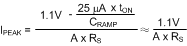
where
- tON is the on-time of the high-side MOSFET
The 1.1-V threshold is the difference between the 1.6-V reference at the current limit comparator and the 0.5-V offset at the current sense amplifier. This offset at the current sense amplifier allows the inductor ripple current to go negative by 0.5 V / (A ✕ RS) when running full synchronous operation.
Current limit hysteresis prevents chatter around the threshold when VCCX is powered from VOUT. When 4.5 V < VCC < 5.8 V, the 1.6-V reference is increased to 1.72 V. The peak current which triggers the current limit comparator becomes:
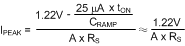
This has the effect of a 10% fold-back of the peak current during a short circuit when VCCX is powered from a 5-V output.