SNVSCU2B August 2024 – August 2025 LM5137-Q1
PRODUCTION DATA
- 1
- 1 Features
- 2 Applications
- 3 Description
- 4 Related Products
- 5 Pin Configuration and Functions
- 6 Specifications
-
7 Detailed Description
- 7.1 Overview
- 7.2 Functional Block Diagram
- 7.3
Feature Description
- 7.3.1 Input Voltage Range (VIN)
- 7.3.2 Bias Supply Regulator (VCC, BIAS1/VOUT1, VDDA)
- 7.3.3 Precision Enable (EN1, EN2)
- 7.3.4 Switching Frequency (RT)
- 7.3.5 Pulse Frequency Modulation and Synchronization (PFM/SYNC)
- 7.3.6 Synchronization Out (SYNCOUT)
- 7.3.7 Dual Random Spread Spectrum (DRSS)
- 7.3.8 Configurable Soft Start (RSS)
- 7.3.9 Output Voltage Setpoints (FB1, FB2)
- 7.3.10 Error Amplifier and PWM Comparator (FB1, FB2, COMP1, COMP2)
- 7.3.11 Inductor Current Sense (ISNS1+, BIAS1/VOUT1, ISNS2+, VOUT2)
- 7.3.12 Minimum Controllable On-Time
- 7.3.13 100% Duty Cycle Capability
- 7.3.14 MOSFET Gate Drivers (HO1, HO2, LO1, LO2)
- 7.3.15 Output Configurations (CNFG)
- 7.4 Device Functional Modes
-
8 Application and Implementation
- 8.1 Application Information
- 8.2
Typical Applications
- 8.2.1
Design 1 – Dual 5V and 3.3V, 20A Buck Regulator for 12V
Automotive Battery Applications
- 8.2.1.1 Design Requirements
- 8.2.1.2
Detailed Design Procedure
- 8.2.1.2.1 Custom Design With WEBENCH® Tools
- 8.2.1.2.2 Custom Design With Excel Quickstart Tool
- 8.2.1.2.3 Inductor Calculations
- 8.2.1.2.4 Shunt Resistors
- 8.2.1.2.5 Ceramic Output Capacitors
- 8.2.1.2.6 Ceramic Input Capacitors
- 8.2.1.2.7 Feedback Resistors
- 8.2.1.2.8 Input Voltage UVLO Resistors
- 8.2.1.2.9 Compensation Components
- 8.2.1.3 Application Curves
- 8.2.2 Design 2 – Two-Phase, Single-Output Synchronous Buck Regulator for Automotive ADAS Applications
- 8.2.3 Design 3 – 12V, 20A, 400kHz, Two-Phase Buck Regulator for 48V Automotive Applications
- 8.2.1
Design 1 – Dual 5V and 3.3V, 20A Buck Regulator for 12V
Automotive Battery Applications
- 8.3 Power Supply Recommendations
- 8.4 Layout
- 9 Device and Documentation Support
- 10Revision History
- 11Mechanical, Packaging, and Orderable Information
Package Options
Mechanical Data (Package|Pins)
- RHA|36
Thermal pad, mechanical data (Package|Pins)
- RHA|36
Orderable Information
7.3.9 Output Voltage Setpoints (FB1, FB2)
The LM5137-Q1 can be independently configured for one of the three fixed output voltage setpoints or adjusted to the desired output voltage using an external resistor divider. As shown in Table 7-2, configure VOUT1 or VOUT2 for a 3.3V, 5V, or 12V voltage setpoint by connecting the respective FB pin with a 7.5kΩ, 24.9kΩ, or 48.7kΩ to VDDA, respectively.
| PULLUP RESISTOR TO VDDA | VOUT SETPOINT |
|---|---|
| 7.5kΩ | 3.3V |
| 24.9kΩ | 5V |
| 48.7kΩ | 12V |
| Not installed | External FB divider setting |
The configuration settings are latched and cannot be changed until the LM5137-Q1 is powered down with the VCC voltage decreasing below the falling UVLO threshold, and then powered up again with VCC above 3.8V.
Alternatively, set the output voltage with an external resistor divider from the output to AGND. The FB regulation voltage is 0.8V, and the output voltage setpoint range is from 0.8V to 60V. Use Equation 4 to calculate the upper and lower feedback resistors, designated RFB1 and RFB2, respectively. See Figure 7-4.
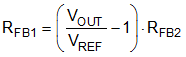
A recommended starting value for RFB2 is between 10kΩ and 20kΩ.
 Figure 7-4 Voltage
Loop With Adjustable Output Setting
Figure 7-4 Voltage
Loop With Adjustable Output SettingIf high light-load efficiency is required, take care when selecting the external resistors. The current consumption of the external divider adds to the LM5137-Q1 sleep current. The divider current reflected to VIN scales by the ratio of VOUT/VIN.