SNVSB32B August 2018 – June 2021 LM5146-Q1
PRODUCTION DATA
- 1 Features
- 2 Applications
- 3 Description
- 4 Revision History
- 5 Description (continued)
- 6 Pin Configuration and Functions
- 7 Specifications
-
8 Detailed Description
- 8.1 Overview
- 8.2 Functional Block Diagram
- 8.3
Feature Description
- 8.3.1 Input Range (VIN)
- 8.3.2 Output Voltage Setpoint and Accuracy (FB)
- 8.3.3 High-Voltage Bias Supply Regulator (VCC)
- 8.3.4 Precision Enable (EN/UVLO)
- 8.3.5 Power Good Monitor (PGOOD)
- 8.3.6 Switching Frequency (RT, SYNCIN)
- 8.3.7 Configurable Soft Start (SS/TRK)
- 8.3.8 Voltage-Mode Control (COMP)
- 8.3.9 Gate Drivers (LO, HO)
- 8.3.10 Current Sensing and Overcurrent Protection (ILIM)
- 8.3.11 OCP Duty Cycle Limiter
- 8.4 Device Functional Modes
- 9 Application and Implementation
- 10Power Supply Recommendations
- 11Layout
- 12Device and Documentation Support
- 13Mechanical, Packaging, and Orderable Information
Package Options
Refer to the PDF data sheet for device specific package drawings
Mechanical Data (Package|Pins)
- RGY|20
Thermal pad, mechanical data (Package|Pins)
- RGY|20
Orderable Information
8.3.10 Current Sensing and Overcurrent Protection (ILIM)
The LM5146-Q1 implements a lossless current sense scheme designed to limit the inductor current during an overload or short-circuit condition. Figure 8-8 portrays the popular current sense method using the on-state resistance of the low-side MOSFET. Meanwhile, Figure 8-9 shows an alternative implementation with current shunt resistor, RS. The LM5146-Q1 senses the inductor current during the PWM off-time (when LO is high).
 Current Sensing") Figure 8-8 MOSFET RDS(on) Current Sensing
Figure 8-8 MOSFET RDS(on) Current Sensing Figure 8-9 Shunt Resistor Current Sensing
The ILIM pin of the LM5146-Q1 sources a reference current that flows in an external resistor, designated RILIM, to program of the current limit threshold. A current limit comparator on the ILIM pin prevents further SW pulses if the ILIM pin voltage goes below GND. Figure 8-10 shows the implementation.
Resistor RILIM is tied to SW to use the RDS(on) of the low-side MOSFET as a sensing element (termed RDS(on) mode). Alternatively, RILIM is tied to a shunt resistor connected at the source of the low-side MOSFET (termed RSENSE mode). The LM5146-Q1 detects the appropriate mode at start-up and sets the source current amplitude and temperature coefficient (TC) accordingly.
The ILIM current with RDS-ON sensing is 200 µA at 27°C junction temperature and incorporates a TC of +4500 ppm/°C to generally track the RDS(on) temperature variation of the low-side MOSFET. Conversely, the ILIM current is a constant 100 µA in RSENSE mode. This controls the valley of the inductor current during a steady-state overload at the output. Depending on the chosen mode, select the resistance of RILIM using Equation 6.
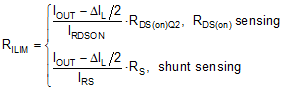
where
- ΔIL is the peak-to-peak inductor ripple current
- RDS(on)Q2 is the on-state resistance of the low-side MOSFET
- IRDSON is the ILIM pin current in RDS-ON mode
- RS is the resistance of the current-sensing shunt element
- IRS is the ILIM pin current in RSENSE mode
Given the large voltage swings of ILIM in RDS(on) sensing mode, a capacitor designated CILIM connected from ILIM to PGND is essential to the operation of the valley current limit circuit. Choose this capacitance such that the time constant RILIM· CILIM is approximately 6 ns.
 Figure 8-10 OCP Setpoint Defined by Current Source IRDSON and Resistor RILIM in RDS-ON Mode
Note that current sensing with a shunt component is typically implemented at lower output current levels to provide accurate overcurrent protection. Burdened by the unavoidable efficiency penalty, PCB layout, and additional cost implications, this configuration is not usually implemented in high-current applications (except where OCP setpoint accuracy and stability over the operating temperature range are critical specifications).