SNVSB32B August 2018 – June 2021 LM5146-Q1
PRODUCTION DATA
- 1 Features
- 2 Applications
- 3 Description
- 4 Revision History
- 5 Description (continued)
- 6 Pin Configuration and Functions
- 7 Specifications
-
8 Detailed Description
- 8.1 Overview
- 8.2 Functional Block Diagram
- 8.3
Feature Description
- 8.3.1 Input Range (VIN)
- 8.3.2 Output Voltage Setpoint and Accuracy (FB)
- 8.3.3 High-Voltage Bias Supply Regulator (VCC)
- 8.3.4 Precision Enable (EN/UVLO)
- 8.3.5 Power Good Monitor (PGOOD)
- 8.3.6 Switching Frequency (RT, SYNCIN)
- 8.3.7 Configurable Soft Start (SS/TRK)
- 8.3.8 Voltage-Mode Control (COMP)
- 8.3.9 Gate Drivers (LO, HO)
- 8.3.10 Current Sensing and Overcurrent Protection (ILIM)
- 8.3.11 OCP Duty Cycle Limiter
- 8.4 Device Functional Modes
- 9 Application and Implementation
- 10Power Supply Recommendations
- 11Layout
- 12Device and Documentation Support
- 13Mechanical, Packaging, and Orderable Information
Package Options
Refer to the PDF data sheet for device specific package drawings
Mechanical Data (Package|Pins)
- RGY|20
Thermal pad, mechanical data (Package|Pins)
- RGY|20
Orderable Information
9.1.2.4 Power MOSFETs
The choice of power MOSFETs has significant impact on DC/DC regulator performance. A MOSFET with low on-state resistance, RDS(on), reduces conduction loss, whereas low parasitic capacitances enable faster transition times and reduced switching loss. Normally, the lower the RDS(on) of a MOSFET, the higher the gate charge and output charge (QG and QOSS respectively), and vice versa. As a result, the product RDS(on) × QG is commonly specified as a MOSFET figure-of-merit. Low thermal resistance ensures that the MOSFET power dissipation does not result in excessive MOSFET die temperature.
The main parameters affecting power MOSFET selection in a LM5146-Q1 application are as follows:
- RDS(on) at VGS = 7.5 V
- Drain-source voltage rating, BVDSS, typically 60 V, 80 V, or 100 V, depending on maximum input voltage
- Gate charge parameters at VGS = 7.5 V
- Output charge, QOSS, at the relevant input voltage
- Body diode reverse recovery charge, QRR
- Gate threshold voltage, VGS(th), derived from the Miller plateau evident in the QG versus VGS plot in the MOSFET data sheet. With a Miller plateau voltage typically in the range of 2 V to 5 V, the 7.5-V gate drive amplitude of the LM5146-Q1 provides an adequately-enhanced MOSFET when on and a margin against Cdv/dt shoot-through when off.
The MOSFET-related power losses are summarized by the equations presented in Table 9-1, where suffixes 1 and 2 represent high-side and low-side MOSFET parameters, respectively. While the influence of inductor ripple current is considered, second-order loss modes, such as those related to parasitic inductances and SW node ringing, are not included. Consult the LM5146-Q1 Quickstart Calculator to assist with power loss calculations.
| POWER LOSS MODE | HIGH-SIDE MOSFET | LOW-SIDE MOSFET |
|---|---|---|
| MOSFET conduction(2)(3) | 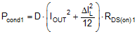 | 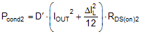 |
| MOSFET switching | 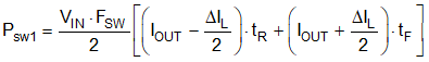 | Negligible |
| MOSFET gate drive(1) | 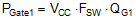 | 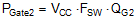 |
| MOSFET output charge(4) |  | |
| Body diode conduction | N/A | 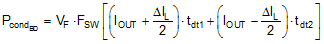 |
| Body diode reverse recovery(5) |  | |
The high-side (control) MOSFET carries the inductor current during the PWM on-time (or D interval) and typically incurs most of the switching losses. It is therefore imperative to choose a high-side MOSFET that balances conduction and switching loss contributions. The total power dissipation in the high-side MOSFET is the sum of the losses due to conduction, switching (voltage-current overlap), output charge, and typically two-thirds of the net loss attributed to body diode reverse recovery.
The low-side (synchronous) MOSFET carries the inductor current when the high-side MOSFET is off (or 1–D interval). The low-side MOSFET switching loss is negligible as it is switched at zero voltage – current just commutates from the channel to the body diode or vice versa during the transition deadtimes. The LM5146-Q1, with its adaptive gate drive timing, minimizes body diode conduction losses when both MOSFETs are off. Such losses scale directly with switching frequency.
In high step-down ratio applications, the low-side MOSFET carries the current for a large portion of the switching period. Therefore, to attain high efficiency, it is critical to optimize the low-side MOSFET for low RDS(on). In cases where the conduction loss is too high or the target RDS(on) is lower than available in a single MOSFET, connect two low-side MOSFETs in parallel. The total power dissipation of the low-side MOSFET is the sum of the losses due to channel conduction, body diode conduction, and typically one-third of the net loss attributed to body diode reverse recovery. The LM5146-Q1 is well suited to drive TI's portfolio of NexFET™ power MOSFETs.