SNVSAE4C July   2015  – October 2018 LM5160-Q1

PRODUCTION DATA.  

  1. Features
  2. Applications
  3. Description
    1.     Device Images
      1.      Typical Synchronous Buck Application Circuit
      2.      Typical Fly-Buck Application Circuit
  4. Revision History
  5. Pin Configuration and Functions
    1.     Pin Functions
  6. Specifications
    1. 6.1 Absolute Maximum Ratings
    2. 6.2 ESD Ratings
    3. 6.3 Recommended Operating Conditions
    4. 6.4 Thermal Information
    5. 6.5 Electrical Characteristics
    6. 6.6 Switching Characteristics
    7. 6.7 Typical Characteristics
  7. Detailed Description
    1. 7.1 Overview
    2. 7.2 Functional Block Diagram
    3. 7.3 Feature Description
      1. 7.3.1  Control Circuit
      2. 7.3.2  VCC Regulator
      3. 7.3.3  Regulation Comparator
      4. 7.3.4  Soft Start
      5. 7.3.5  Error Amplifier
      6. 7.3.6  On-Time Generator
      7. 7.3.7  Current Limit
      8. 7.3.8  N-Channel Buck Switch and Driver
      9. 7.3.9  Synchronous Rectifier
      10. 7.3.10 Enable / Undervoltage Lockout (EN/UVLO)
      11. 7.3.11 Thermal Protection
    4. 7.4 Device Functional Modes
      1. 7.4.1 Forced Pulse Width Modulation (FPWM) Mode
      2. 7.4.2 Undervoltage Detector
  8. Application and Implementation
    1. 8.1 Application Information
      1. 8.1.1 Ripple Configuration
    2. 8.2 Typical Applications
      1. 8.2.1 LM5160-Q1 Synchronous Buck (10-V to 60-V Input, 5-V Output, 1.5-A Load)
        1. 8.2.1.1 Design Requirements
        2. 8.2.1.2 Detailed Design Procedure
          1. 8.2.1.2.1  Custom Design With WEBENCH® Tools
          2. 8.2.1.2.2  Feedback Resistor Divider - RFB1, RFB2
          3. 8.2.1.2.3  Switching Frequency - RON
          4. 8.2.1.2.4  Inductor - L
          5. 8.2.1.2.5  Output Capacitor - COUT
          6. 8.2.1.2.6  Series Ripple Resistor - RESR
          7. 8.2.1.2.7  VCC and Bootstrap Capacitors - CVCC, CBST
          8. 8.2.1.2.8  Input Capacitor - CIN
          9. 8.2.1.2.9  Soft-Start Capacitor - CSS
          10. 8.2.1.2.10 EN/UVLO Resistors - RUV1, RUV2
        3. 8.2.1.3 Application Curves
      2. 8.2.2 LM5160-Q1 Isolated Fly-Buck (18-V to 32-V Input, 12-V, 4.5-W Isolated Output)
        1. 8.2.2.1 LM5160-Q1 Fly-Buck Design Requirements
        2. 8.2.2.2 Detailed Design Procedure
          1. 8.2.2.2.1 Selection of VOUT1 and Turns Ratio
          2. 8.2.2.2.2 Secondary Rectifier Diode
          3. 8.2.2.2.3 External Ripple Circuit
          4. 8.2.2.2.4 Output Capacitor - COUT2
        3. 8.2.2.3 Application Curves
    3. 8.3 Do's and Don'ts
  9. Power Supply Recommendations
  10. 10Layout
    1. 10.1 Layout Guidelines
    2. 10.2 Layout Example
  11. 11Device and Documentation Support
    1. 11.1 Device Support
      1. 11.1.1 Third-Party Products Disclaimer
      2. 11.1.2 Development Support
        1. 11.1.2.1 Custom Design With WEBENCH® Tools
    2. 11.2 Documentation Support
      1. 11.2.1 Related Documentation
    3. 11.3 Receiving Notification of Documentation Updates
    4. 11.4 Community Resources
    5. 11.5 Trademarks
    6. 11.6 Electrostatic Discharge Caution
    7. 11.7 Glossary
  12. 12Mechanical, Packaging, and Orderable Information

Package Options

Mechanical Data (Package|Pins)
Thermal pad, mechanical data (Package|Pins)
Orderable Information

LM5160-Q1 Isolated Fly-Buck (18-V to 32-V Input, 12-V, 4.5-W Isolated Output)

LM5160-Q1 PowerHouseBanner_nvsat9.gif
For technical solutions, industry trends, and insights for designing and managing power supplies, please refer to TI's Power House blog series.

Below is an application example of an isolated Fly-Buck converter that operates over an input voltage range of 18 V to 32 V. It provides a stable 12-V isolated output voltage with an output power capability of 4.5 W. Figure 28 shows the complete schematic of the Fly-Buck application circuit.
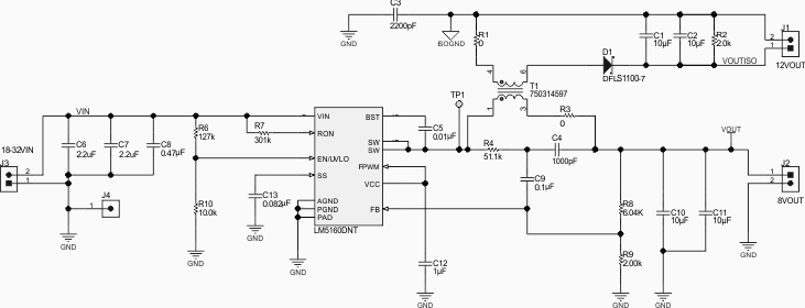
LM5160-Q1 FlyBuck_App_Schematic_SNVSA03.pngFigure 28. LM5160-Q1 12-V, 4.5-W Fly-Buck Converter Schematic