SNOSB22C October 2008 – October 2014 LM5574-Q1
PRODUCTION DATA.
- 1 Features
- 2 Applications
- 3 Description
- 4 Revision History
- 5 Pin Configuration and Functions
- 6 Specifications
- 7 Detailed Description
- 8 Application and Implementation
- 9 Power Supply Recommendations
- 10Layout
- 11Device and Documentation Support
- 12Mechanical, Packaging, and Orderable Information
Package Options
Mechanical Data (Package|Pins)
- PW|16
Thermal pad, mechanical data (Package|Pins)
Orderable Information
6 Specifications
6.1 Absolute Maximum Ratings(1)(2)
| MIN | MAX | UNIT | ||
|---|---|---|---|---|
| VIN to GND | 76 | V | ||
| BST to GND | 90 | V | ||
| PRE to GND | 76 | V | ||
| SW to GND (Steady State) | –1.5 | V | ||
| BST to VCC | 76 | V | ||
| SD, VCC to GND | 14 | V | ||
| BST to SW | 14 | V | ||
| OUT to GND | Limited to VIN | |||
| SYNC, SS, FB, RAMP to GND | 7 | V | ||
6.2 Handling Ratings
| MIN | MAX | UNIT | |||
|---|---|---|---|---|---|
| Tstg | Storage temperature range | –65 | 150 | °C | |
| V(ESD) | Electrostatic discharge | Human body model (HBM), per ANSI/ESDA/JEDEC JS-001, all pins(1) | 2 | kV | |
(1) JEDEC document JEP155 states that 500-V HBM allows safe manufacturing with a standard ESD control process.
6.3 Recommended Operating Conditions
| MIN | MAX | UNIT | |
|---|---|---|---|
| VIN | 6 | 75 | V |
| Operation Junction Temperature | –40 | 150 | °C |
6.4 Thermal Information
| THERMAL METRIC(1) | LM5574-Q1 | UNIT | |
|---|---|---|---|
| PW | |||
| 16 PINS | |||
| RθJA | Junction-to-ambient thermal resistance | 90 | °C/W |
| RθJC(top) | Junction-to-case (top) thermal resistance | 30 | |
(1) For more information about traditional and new thermal metrics, see the IC Package Thermal Metrics application report, SPRA953.
6.5 Electrical Characteristics
VIN = 48V, RT = 32.4kΩ, typical values correspond to TJ = 25°C. Minimum and maximum limits apply over -40°C to 125°C junction temperature range unless otherwise stated.| PARAMETER | TEST CONDITIONS | MIN | TYP | MAX | UNIT | |
|---|---|---|---|---|---|---|
| STARTUP REGULATOR | ||||||
| VCCReg | VCC Regulator Output | 6.85 | 7.15 | 7.5 | V | |
| VCC LDO Mode turn-off | 9 | V | ||||
| VCC Current Limit | VCC = 0 V | 25 | mA | |||
| VCC SUPPLY | ||||||
| VCC UVLO Threshold | (VCC increasing) | 5.01 | 5.35 | 5.69 | V | |
| VCC Undervoltage Hysteresis | 0.35 | V | ||||
| Bias Current (Iin) | FB = 1.3 V | 3.7 | 4.5 | mA | ||
| Shutdown Current (Iin) | SD = 0 V | 57 | 85 | µA | ||
| SHUTDOWN THRESHOLDS | ||||||
| Shutdown Threshold | (SD Increasing) | 0.43 | 0.7 | 0.9 | V | |
| Shutdown Hysteresis | 0.1 | V | ||||
| Standby Threshold | (Standby Increasing) | 1.15 | 1.225 | 1.3 | V | |
| Standby Hysteresis | 0.1 | V | ||||
| SD Pull-up Current Source | 5 | µA | ||||
| SWITCH CHARACTERISTICS | ||||||
| Buck Switch Rds(on) | 750 | 1650 | mΩ | |||
| BOOST UVLO | 4 | V | ||||
| BOOST UVLO Hysteresis | 0.56 | V | ||||
| Pre-charge Switch Rds(on) | 70 | Ω | ||||
| Pre-charge Switch on-time | 250 | ns | ||||
| CURRENT LIMIT | ||||||
| Cycle by Cycle Current Limit | RAMP = 0 V | 0.58 | 0.7 | 0.9 | A | |
| Cycle by Cycle Current Limit Delay | RAMP = 2.5 V | 75 | ns | |||
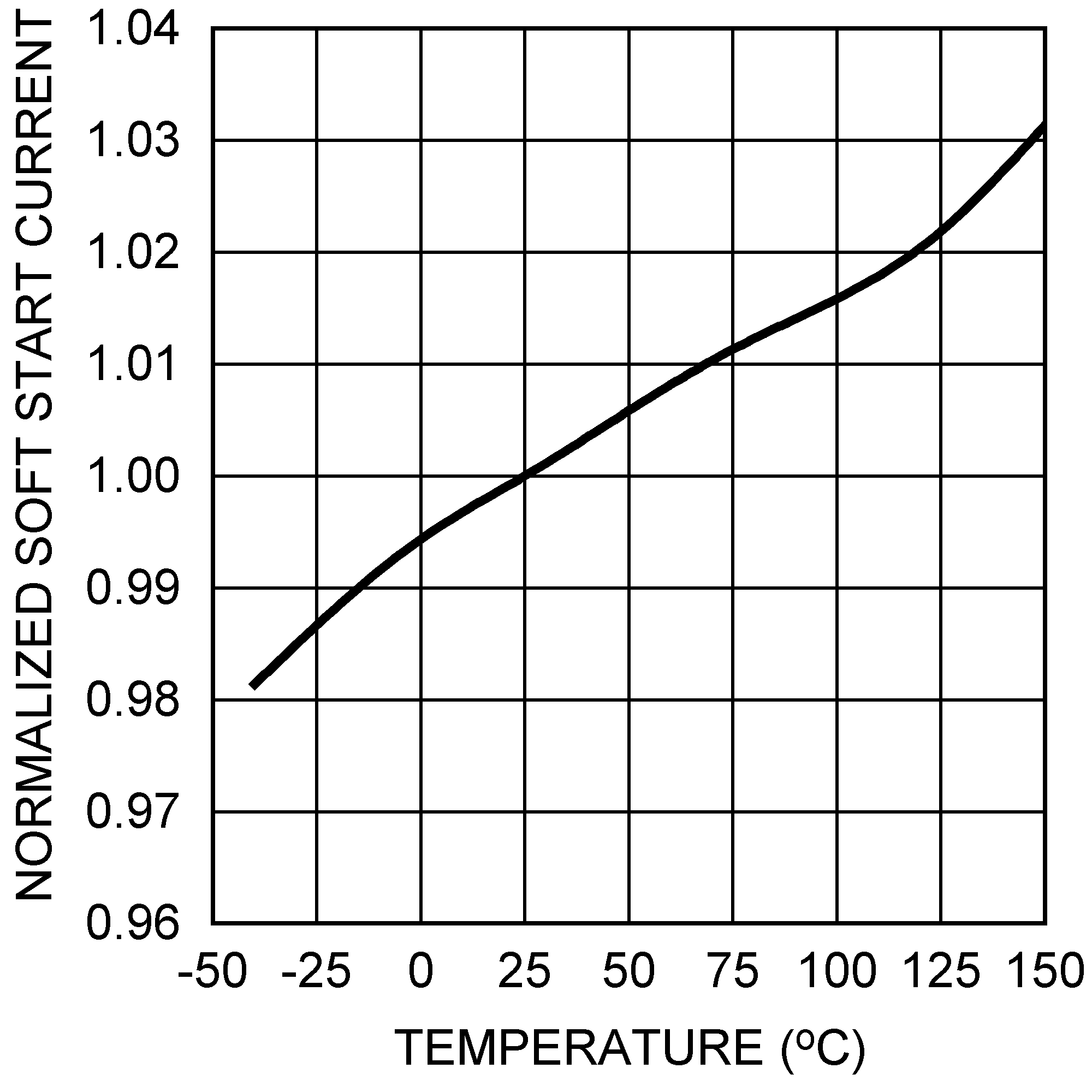
| SOFT-START | ||||||
| SS Current Source | 7 | 10 | 14 | µA | ||
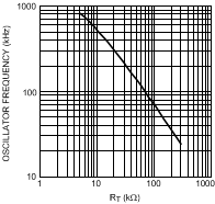
| OSCILLATOR | ||||||
| Frequency1 | 180 | 200 | 220 | kHz | ||
| Frequency2 | RT = 11kΩ | 425 | 485 | 545 | kHz | |
| SYNC Source Impedance | 11 | kΩ | ||||
| SYNC Sink Impedance | 110 | Ω | ||||
| SYNC Threshold (falling) | 1.3 | V | ||||
| SYNC Frequency | RT = 11kΩ | 550 | kHz | |||
| SYNC Pulse Width Minimum | 15 | ns | ||||
| RAMP GENERATOR | ||||||
| Ramp Current 1 | VIN = 60 V, VOUT=10 V | 467 | 550 | 633 | µA | |
| Ramp Current 2 | VIN = 10 V, VOUT=10 V | 36 | 50 | 64 | µA | |
| PWM COMPARATOR | ||||||
| Forced Off-time | 390 | 500 | 590 | ns | ||
| Min On-time | 80 | ns | ||||
| COMP to PWM Comparator Offset | 0.7 | V | ||||
| ERROR AMPLIFIER | ||||||
| Feedback Voltage | Vfb = COMP | 1.205 | 1.225 | 1.245 | V | |
| FB Bias Current | 17 | nA | ||||
| DC Gain | 70 | dB | ||||
| COMP Sink / Source Current | 3 | mA | ||||
| Unity Gain Bandwidth | 3 | MHz | ||||
| DIODE SENSE RESISTANCE | ||||||
| DSENSE | 250 | mΩ | ||||
| THERMAL SHUTDOWN | ||||||
| Tsd | Thermal Shutdown Threshold | 180 | °C | |||
| Thermal Shutdown Hysteresis | 25 | °C | ||||
(1) Absolute Maximum Ratings are limits beyond which damage to the device may occur. Recommended Operating Conditions are conditions under which operation of the device is intended to be functional. For ensured specifications and test conditions, see the Electrical Characteristics.
(2) If Military/Aerospace specified devices are required, please contact the Texas Instruments Sales Office/ Distributors for availability and specifications.
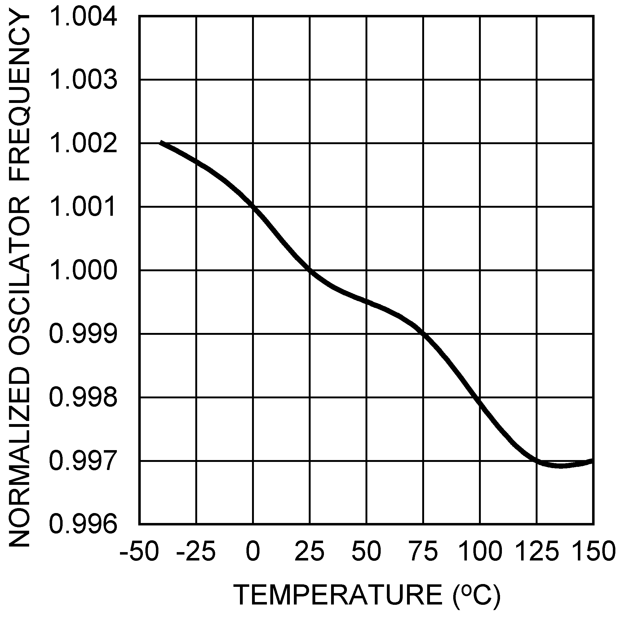
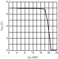
6.6 Typical Characteristics
RL = 7kΩ
FOSC = 200 kHz
VIN = 12 V
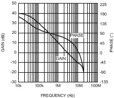
AVCL = 101