SNVSAH5A September   2017  – May 2020 LM73605 , LM73606

PRODUCTION DATA.  

  1. Features
  2. Applications
  3. Description
    1.     Device Images
      1.      Simplified Schematic
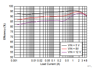
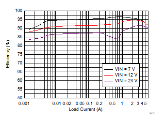
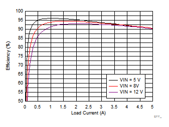
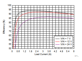
      2.      Efficiency versus Load Current VOUT = 5 V, fSW = 500 kHz, Auto Mode
  4. Revision History
  5. Pin Configuration and Functions
    1.     Pin Functions
  6. Specifications
    1. 6.1 Absolute Maximum Ratings
    2. 6.2 ESD Ratings
    3. 6.3 Recommended Operating Conditions
    4. 6.4 Thermal Information
    5. 6.5 Electrical Characteristics
    6. 6.6 Timing Characteristics
    7. 6.7 Switching Characteristics
    8. 6.8 System Characteristics
    9. 6.9 Typical Characteristics
  7. Detailed Description
    1. 7.1 Overview
    2. 7.2 Functional Block Diagram
    3. 7.3 Feature Description
      1. 7.3.1  Synchronous Step-Down Regulator
      2. 7.3.2  Auto Mode and FPWM Mode
      3. 7.3.3  Fixed-Frequency Peak Current-Mode Control
      4. 7.3.4  Adjustable Output Voltage
      5. 7.3.5  Enable and UVLO
      6. 7.3.6  Internal LDO, VCC_UVLO, and BIAS Input
      7. 7.3.7  Soft Start and Voltage Tracking
      8. 7.3.8  Adjustable Switching Frequency
      9. 7.3.9  Frequency Synchronization and Mode Setting
      10. 7.3.10 Internal Compensation and CFF
      11. 7.3.11 Bootstrap Capacitor and VBOOT-UVLO
      12. 7.3.12 Power-Good and Overvoltage Protection
      13. 7.3.13 Overcurrent and Short-Circuit Protection
      14. 7.3.14 Thermal Shutdown
    4. 7.4 Device Functional Modes
      1. 7.4.1 Shutdown Mode
      2. 7.4.2 Standby Mode
      3. 7.4.3 Active Mode
        1. 7.4.3.1 CCM Mode
        2. 7.4.3.2 DCM Mode
        3. 7.4.3.3 PFM Mode
        4. 7.4.3.4 Fault Protection Mode
  8. Application and Implementation
    1. 8.1 Application Information
    2. 8.2 Typical Application
      1. 8.2.1 Design Requirements
      2. 8.2.2 Detailed Design Procedure
        1. 8.2.2.1  Custom Design With WEBENCH® Tools
        2. 8.2.2.2  Output Voltage Setpoint
        3. 8.2.2.3  Switching Frequency
        4. 8.2.2.4  Input Capacitors
        5. 8.2.2.5  Inductor Selection
        6. 8.2.2.6  Output Capacitor Selection
        7. 8.2.2.7  Feedforward Capacitor
        8. 8.2.2.8  Bootstrap Capacitors
        9. 8.2.2.9  VCC Capacitor
        10. 8.2.2.10 BIAS
        11. 8.2.2.11 Soft Start
        12. 8.2.2.12 Undervoltage Lockout Setpoint
        13. 8.2.2.13 PGOOD
      3. 8.2.3 Application Curves
  9. Power Supply Recommendations
  10. 10Layout
    1. 10.1 Layout Guidelines
      1. 10.1.1 Layout For EMI Reduction
      2. 10.1.2 Ground Plane
      3. 10.1.3 Optimize Thermal Performance
    2. 10.2 Layout Example
  11. 11Device and Documentation Support
    1. 11.1 Device Support
      1. 11.1.1 Third-Party Products Disclaimer
      2. 11.1.2 Development Support
        1. 11.1.2.1 Custom Design With WEBENCH® Tools
    2. 11.2 Documentation Support
      1. 11.2.1 Related Documentation
    3. 11.3 Related Links
    4. 11.4 Receiving Notification of Documentation Updates
    5. 11.5 Support Resources
    6. 11.6 Trademarks
    7. 11.7 Electrostatic Discharge Caution
    8. 11.8 Glossary
  12. 12Mechanical, Packaging, and Orderable Information

Package Options

Mechanical Data (Package|Pins)
Thermal pad, mechanical data (Package|Pins)
Orderable Information

Application Curves

LM73605 LM73606 EFF_3p3V500K_PFM05_SNVSAH5.gif
VOUT = 3.3 V fSW = 500 kHz Auto Mode
Figure 27. LM73605 Efficiency
LM73605 LM73606 EFF_3p3V2p2M_PFM05_SNVSAH5.gif
VOUT = 3.3 V fSW = 2200 kHz Auto Mode
Figure 29. LM73605 Efficiency
LM73605 LM73606 EFF_3p3V350k_PFM05_SNVSAH5.gif
VOUT = 3.3 V fSW = 350 kHz Auto Mode
Figure 31. LM73605 Efficiency
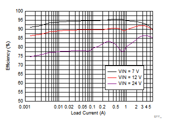
LM73605 LM73606 EFF_5V500K_PFM_SNVSAH5.gif
VOUT = 5 V fSW = 500 kHz Auto Mode
Figure 33. LM73606 Efficiency
LM73605 LM73606 EFF_5V1M_PFM_SNVSAH5.gif
VOUT = 5 V fSW = 1000 kHz Auto Mode
Figure 35. LM73606 Efficiency
LM73605 LM73606 EFF_5V2p2M_PFM_SNVSAH5.gif
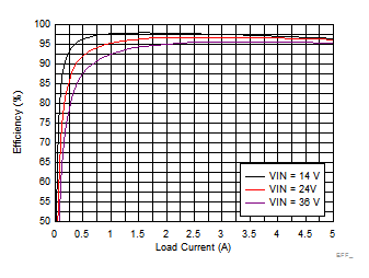
VOUT = 5 V fSW = 2200 kHz Auto Mode
Figure 37. LM73606 Efficiency
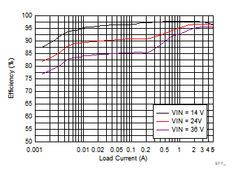
LM73605 LM73606 EFF_12V500K_PFM05_SNVSAH5.gif
VOUT = 12 V fSW = 500 kHz Auto Mode
Figure 39. LM73605 Efficiency
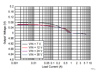
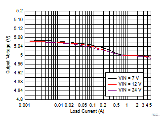
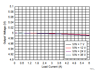
LM73605 LM73606 REG_5V500K_PFM_SNVSAH5.gif
VOUT = 5 V fSW = 500 kHz Auto Mode
Figure 41. LM73606 Load and Line Regulation
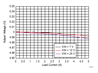
LM73605 LM73606 REG_5V2p2M_PFM05_SNVSAH5.gif
VOUT = 5 V fSW = 2200 kHz Auto Mode
Figure 43. LM73605 Load and Line Regulation
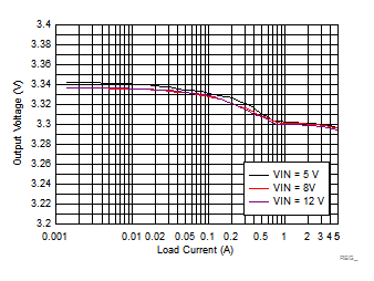
LM73605 LM73606 REG_3p3V2p2M_PFM05_SNVSAH5.gif
VOUT = 3.3 V fSW = 2200 kHz Auto Mode
Figure 45. LM73605 Load and Line Regulation
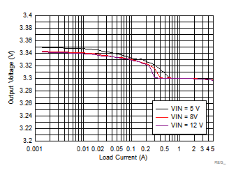
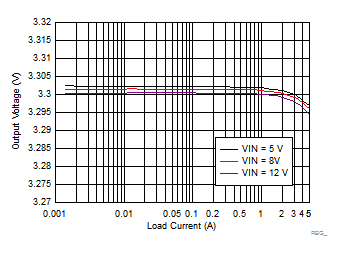
LM73605 LM73606 REG_3p3V500K_PFM05_SNVSAH5.gif
VOUT = 3.3 V fSW = 500 kHz Auto Mode
Figure 47. LM73605 Load and Line Regulation
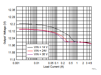
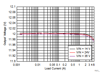
LM73605 LM73606 REG_12V500K_PFM05_SNVSAH5.gif
VOUT = 12 V fSW = 500 kHz Auto Mode
Figure 49. LM73605 Load and Line Regulation
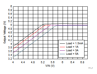
LM73605 LM73606 DO_5V2p2M_PFM05_SNVSAH5.gif
VOUT = 5 V fSW = 2200 kHz Auto Mode
Figure 51. LM73605 Dropout Curve
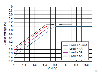
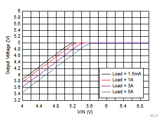
LM73605 LM73606 DO_5V500K_PFM05_SNVSAH5.gif
VOUT = 5 V fSW = 500 kHz Auto Mode
Figure 53. LM73605 Dropout Curve
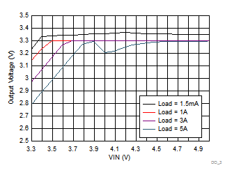
LM73605 LM73606 DO_3p3V500K_PFM05_SNVSAH5.gif
VOUT = 3.3 V fSW = 500 kHz Auto Mode
Figure 55. LM73605 Dropout Curve
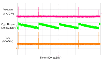
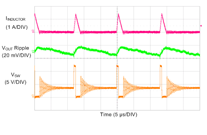
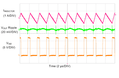
LM73605 LM73606 SCOPE_3p3V_500k_DC_1mA_PFM_SNVSAH5.gif
VIN = 12 V VOUT = 3.3 V fSW = 500 kHz
IOUT = 1 mA Auto Mode
Figure 57. LM73606 Switching Waveform and VOUT Ripple
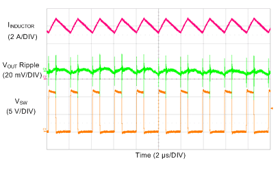
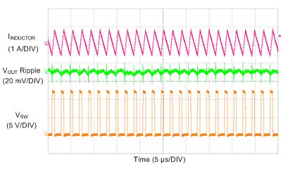
LM73605 LM73606 SCOPE_3p3V_500k_DC_100mA_PFM_SNVSAH5.gif
VIN = 12 V VOUT = 3.3 V fSW = 500 kHz
IOUT = 100 mA Auto Mode
Figure 59. LM73606 Switching Waveform and VOUT Ripple
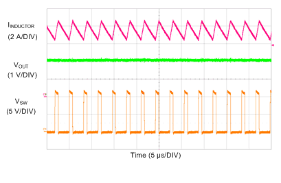
LM73605 LM73606 SCOPE_3p3V_500k_DC_6A_PFM_SNVSAH5.gif
VIN = 12 V VOUT = 3.3 V fSW = 500 kHz
IOUT = 6 A Auto Mode
Figure 61. LM73606 Switching Waveform and VOUT Ripple
LM73605 LM73606 SCOPE_3p3V_500k_OC_7p5A_SNVSAH5.gif
VIN = 12 V VOUT set at 3.3 V fSW set at 500 kHz
IOUT = 7.5 A VOUT droops to 2 V
Figure 63. LM73606 Overcurrent Behavior
LM73605 LM73606 SCOPE_3p3V_500k_SS_200mA_FPWM_SNVSAH5.gif
VIN = 12 V VOUT = 3.3 V fSW = 500 kHz
IOUT= 200 mA FPWM Mode
Figure 65. LM73606 Soft Start With 200-mA Load in FPWM Mode
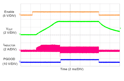
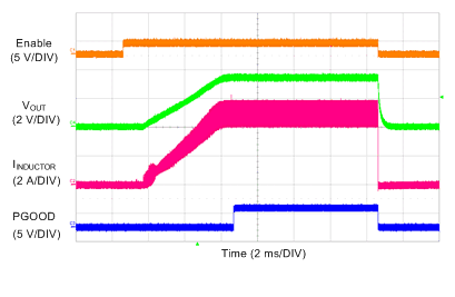
LM73605 LM73606 SCOPE_3p3V_500k_SS_5A_SNVSAH5.gif
VIN = 12 V VOUT = 3.3 V fSW = 500 kHz
IOUT = 5 A Auto Mode
Figure 67. LM73606 Soft Start With 5-A Load
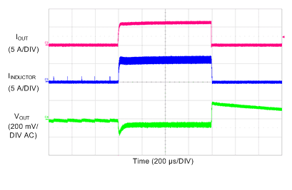
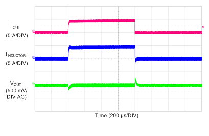
LM73605 LM73606 SCOPE_3p3V_500k_Load_10mA6A_PFM_SNVSAH5.gif
VIN = 12 V VOUT = 3.3 V fSW = 500 kHz
IOUT = 10 mA to 6 A to 10 mA Auto Mode
Figure 69. LM73606 Load Transients
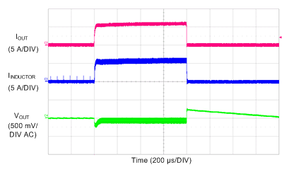
LM73605 LM73606 SCOPE_5V_2p2M_Load_10mA5A_PFM_SNVSAH5.gif
VIN = 12 V VOUT = 5 V fSW = 2200 kHz
IOUT = 10 mA to 5 A to 10 mA Auto Mode
Figure 71. LM73605 Load Transients
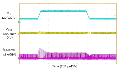
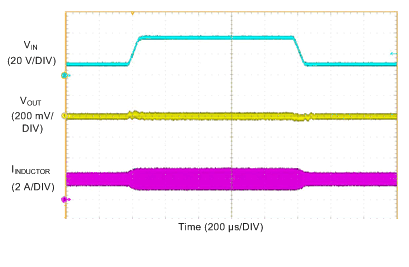
LM73605 LM73606 SCOPE_3p3V_500k_Line10_35_100mA_SNVSAH5.gif
IOUT = 100 mA VOUT = 3.3 V fSW = 500 kHz
VIN = 10 V to 35 V to 10 V Auto Mode
Figure 73. LM73606 Line Transients
LM73605 LM73606 EFF_3p3V500K_FPWM05_SNVSAH5.gif
VOUT = 3.3 V fSW = 500 kHz FPWM Mode
Figure 28. LM73605 Efficiency
LM73605 LM73606 EFF_3p3V2p2M_FPWM05_SNVSAH5.gif
VOUT = 3.3 V fSW = 2200 kHz FPWM Mode
Figure 30. LM73605 Efficiency
LM73605 LM73606 EFF_3p3V1M_PFM05_SNVSAH5.gif
VOUT = 3.3 V fSW = 1000 kHz Auto Mode
Figure 32. LM73605 Efficiency
LM73605 LM73606 EFF_5V500K_FPWM_L_SNVSAH5.gif
VOUT = 5 V fSW = 500 kHz FPWM Mode
Figure 34. LM73606 Efficiency
LM73605 LM73606 EFF_5V1M_FPWM_SNVSAH5.gif
VOUT = 5 V fSW = 1000 kHz FPWM Mode
Figure 36. LM73606 Efficiency
LM73605 LM73606 EFF_5V2p2M_FPWM_SNVSAH5.gif
VOUT = 5 V fSW = 2200 kHz FPWM Mode
Figure 38. LM73606 Efficiency
LM73605 LM73606 EFF_12V500K_FPWM05_SNVSAH5.gif
VOUT = 12 V fSW = 500 kHz FPWM Mode
Figure 40. LM73605 Efficiency
LM73605 LM73606 REG_5V500K_FPWM_SNVSAH5.gif
VOUT = 5 V fSW = 500 kHz FPWM Mode
Figure 42. LM73606 Load and Line Regulation
LM73605 LM73606 REG_5V2p2M_FPWM05_SNVSAH5.gif
VOUT = 5 V fSW = 2200 kHz FPWM Mode
Figure 44. LM73605 Load and Line Regulation
LM73605 LM73606 REG_3p3V2p2M_FPWM05_SNVSAH5.gif
VOUT = 3.3 V fSW = 2200 kHz FPWM Mode
Figure 46. LM73605 Load and Line Regulation
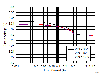
LM73605 LM73606 REG_3p3V1M_PFM05_SNVSAH5.gif
VOUT = 3.3 V fSW = 1000 kHz Auto Mode
Figure 48. LM73605 Load and Line Regulation
LM73605 LM73606 REG_12V500K_FPWM05_SNVSAH5.gif
VOUT = 12 V fSW = 500 kHz FPWM Mode
Figure 50. LM73605 Load and Line Regulation
LM73605 LM73606 DO_5V2p2M_FPWM05_SNVSAH5.gif
VOUT = 5 V fSW = 2200 kHz FPWM Mode
Figure 52. LM73605 Dropout Curve
LM73605 LM73606 DO_5V1M_PFM05_SNVSAH5.gif
VOUT = 5 V fSW = 1000 kHz Auto Mode
Figure 54. LM73605 Dropout Curve
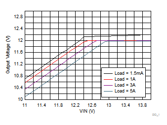
LM73605 LM73606 DO_12V500K_PFM05_SNVSAH5.gif
VOUT = 12 V fSW = 500 kHz Auto Mode
Figure 56. LM73605 Dropout Curve
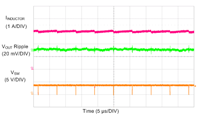
LM73605 LM73606 SCOPE_3p3V_500k_DC_1mA_FPWM_SNVSAH5.gif
VIN = 12 V VOUT = 3.3 V fSW = 500 kHz
IOUT = 1 mA FPWM Mode
Figure 58. LM73606 Switching Waveform and VOUT Ripple
LM73605 LM73606 SCOPE_3p3V_500k_DC_100mA_FPWM_SNVSAH5.gif
VIN = 12 V VOUT = 3.3 V fSW = 500 kHz
IOUT = 100 mA FPWM Mode
Figure 60. LM73606 Switching Waveform and VOUT Ripple
LM73605 LM73606 SCOPE_3p3V_500k_DC_3A_DO_SNVSAH5.gif
VIN = 3.66 V VOUT = 3.3 V fSW set at 500 kHz
IOUT = 3 A Auto Mode
Figure 62. LM73606 Switching Waveform at Dropout
LM73605 LM73606 SCOPE_3p3V_500k_SC_SNVSAH5.gif
VIN = 12 V VOUT = 3.3 V fSW = 500 kHz
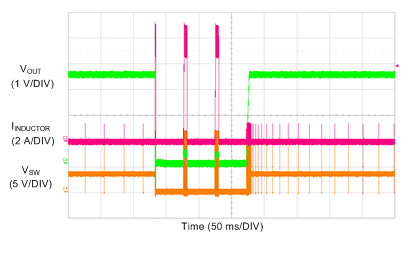
Figure 64. LM73606 Short-Circuit Hiccup Protection and Recovery
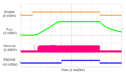
LM73605 LM73606 SCOPE_3p3V_500k_SS_200mA_PFM_SNVSAH5.gif
VIN = 12 V VOUT = 3.3 V fSW = 500 kHz
IOUT= 200 mA Auto Mode
Figure 66. LM73606 Soft Start With 200-mA Load in Auto Mode
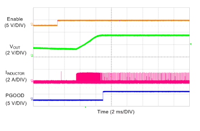
LM73605 LM73606 SCOPE_3p3V_500k_SS_PreB_SNVSAH5.gif
VIN = 12 V VOUT = 3.3 V fSW = 500 kHz
VPRE-BIAS= 1.5 V Auto Mode
Figure 68. LM73606 Soft Start With Pre-Biased Output Voltage
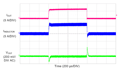
LM73605 LM73606 SCOPE_3p3V_500k_Load_10mA6A_FPWM_SNVSAH5.gif
VIN = 12 V VOUT = 3.3 V fSW = 500 kHz
IOUT = 10 mA to 6 A to 10 mA FPWM Mode
Figure 70. LM73606 Load Transients
LM73605 LM73606 SCOPE_5V_2p2M_Load_10mA5A_FPWM_SNVSAH5.gif
VIN = 12 V VOUT = 5 V fSW = 2200 kHz
IOUT = 10 mA to 5 A to 10 mA FPWM Mode
Figure 72. LM73605 Load Transients
LM73605 LM73606 SCOPE_3p3V_500k_Line10_35_2A_SNVSAH5.gif
IOUT = 2 A VOUT = 3.3 V fSW = 500 kHz
VIN = 10 V to 35 V to 10 V Auto Mode
Figure 74. LM73606 Line Transients