SNVSAH5A September 2017 – May 2020 LM73605 , LM73606
PRODUCTION DATA.
- 1 Features
- 2 Applications
- 3 Description
- 4 Revision History
- 5 Pin Configuration and Functions
- 6 Specifications
-
7 Detailed Description
- 7.1 Overview
- 7.2 Functional Block Diagram
- 7.3
Feature Description
- 7.3.1 Synchronous Step-Down Regulator
- 7.3.2 Auto Mode and FPWM Mode
- 7.3.3 Fixed-Frequency Peak Current-Mode Control
- 7.3.4 Adjustable Output Voltage
- 7.3.5 Enable and UVLO
- 7.3.6 Internal LDO, VCC_UVLO, and BIAS Input
- 7.3.7 Soft Start and Voltage Tracking
- 7.3.8 Adjustable Switching Frequency
- 7.3.9 Frequency Synchronization and Mode Setting
- 7.3.10 Internal Compensation and CFF
- 7.3.11 Bootstrap Capacitor and VBOOT-UVLO
- 7.3.12 Power-Good and Overvoltage Protection
- 7.3.13 Overcurrent and Short-Circuit Protection
- 7.3.14 Thermal Shutdown
- 7.4 Device Functional Modes
-
8 Application and Implementation
- 8.1 Application Information
- 8.2
Typical Application
- 8.2.1 Design Requirements
- 8.2.2
Detailed Design Procedure
- 8.2.2.1 Custom Design With WEBENCH® Tools
- 8.2.2.2 Output Voltage Setpoint
- 8.2.2.3 Switching Frequency
- 8.2.2.4 Input Capacitors
- 8.2.2.5 Inductor Selection
- 8.2.2.6 Output Capacitor Selection
- 8.2.2.7 Feedforward Capacitor
- 8.2.2.8 Bootstrap Capacitors
- 8.2.2.9 VCC Capacitor
- 8.2.2.10 BIAS
- 8.2.2.11 Soft Start
- 8.2.2.12 Undervoltage Lockout Setpoint
- 8.2.2.13 PGOOD
- 8.2.3 Application Curves
- 9 Power Supply Recommendations
- 10Layout
- 11Device and Documentation Support
- 12Mechanical, Packaging, and Orderable Information
Package Options
Mechanical Data (Package|Pins)
- RNP|30
Thermal pad, mechanical data (Package|Pins)
- RNP|30
Orderable Information
10.2 Layout Example
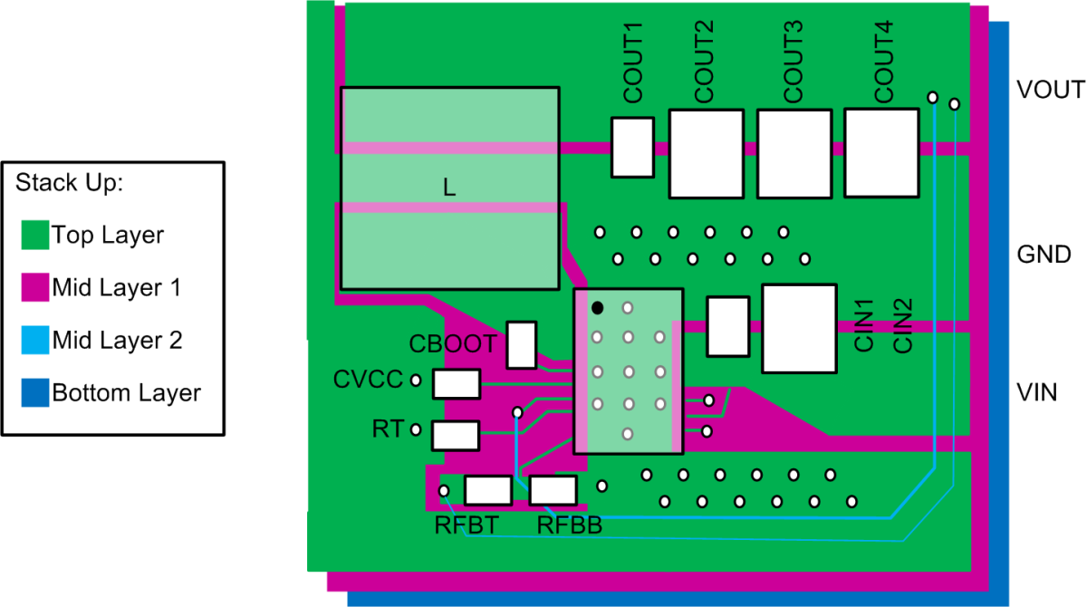
A layout example is shown in Figure 77. A four-layer board is used with 2-oz copper on the top and bottom layers and 1-oz copper on the inner two layers. Figure 77 shows the relative scale of the LM73605 and LM73606 with 0805 and 1210 input and output capacitors, 7-mm × 7-mm inductor and 0603 case size for all other passive components. The trace width of the signal connections are not to scale.
The components are placed on the top layer and the high current paths are routed on the top layer as well. The remaining space on the top layer can be filled with GND polygon. Thermal vias are used under the DAP and around the device. The GND copper was extended to the outside of the device, which serves as copper heat sink.
The mid-layer 1 is right underneath the top layer. It is a solid ground plane, which serves as noise shielding and heat dissipation path.
The VOUT sense trace is routed on the third layer, which is mid-layer 2. Ground plane provided noise shielding for the sense trace. The VOUT to BIAS connection is routed by a separate trace.
The bottom layer is also a solid ground copper in this example. Solid copper provides best heat sinking for the device. If components and traces need to be on the bottom layer, leave the area around thermal vias as solid as possible. Try not to cut heat dissipation path by a trace. The board can be used for various frequencies and output voltages, with component variation. For more details, see the LM73605/LM73606 EVM User's Guide.
 Figure 77. LM73605 and LM73606 Layout Example