SNOSDD6 September 2021 LM74700-EP
PRODUCTION DATA
- 1 Features
- 2 Applications
- 3 Description
- 4 Revision History
- 5 Pin Configuration and Functions
- 6 Specifications
- 7 Parameter Measurement Information
- 8 Detailed Description
-
9 Application and Implementation
- 9.1 Application Information
- 9.2 Typical Application
- 9.3 OR-ing Application Configuration
- 10Power Supply Recommendations
- 11Layout
- 12Device and Documentation Support
- 13Mechanical, Packaging, and Orderable Information
Package Options
Mechanical Data (Package|Pins)
- DDF|8
Thermal pad, mechanical data (Package|Pins)
Orderable Information
9.2.4 Selection of TVS Diodes and MOSFET for 24-V Battery Protection Applications
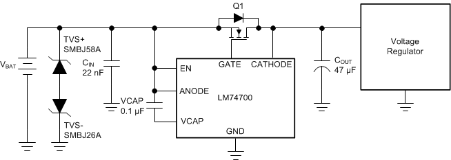
Typical 24-V battery protection application circuit shown in Figure 9-3 uses two uni-directional TVS diodes to protect from positive and negative transient voltages.
 Figure 9-3 Typical 24-V Battery
Protection With Two Uni-directional TVS
Figure 9-3 Typical 24-V Battery
Protection With Two Uni-directional TVSThe breakdown voltage of the TVS+ must be higher than 48-V jump start voltage, less than the absolute maximum ratings of anode and enable pin of LM74700-EP (65 V) and must withstand 65-V suppressed load dump. The breakdown voltage of TVS– must be lower than maximum reverse battery voltage –32 V, so that the TVS– is not damaged due to long time exposure to reverse connected battery.
During ISO 7637-2 pulse 1, the input voltage goes up to –600 V with a generator impedance of 50 Ω. This action translates to 12 A flowing through the TVS–. The clamping voltage of the TVS- cannot be same as that of 12-V battery protection circuit. Because during the ISO 7637-2 pulse, the Anode to Cathode voltage seen is equal to (– TVS Clamping voltage + Output capacitor voltage). For 24-V battery application, the maximum battery voltage is 32 V, then the clamping voltage of the TVS– must not exceed 75 V – 32 V = 43 V.
Single bi-directional TVS cannot be used for 24-V battery protection because breakdown voltage for TVS+ ≥ 65 V, maximum clamping voltage is ≤ 43 V and the clamping voltage cannot be less than the breakdown voltage. Two un-directional TVS connected back-to-back needs to be used at the input. For positive side TVS+, SMBJ58A with the breakdown voltage of 64.4 V (minimum), 67.8 (typical) is recommended. For the negative side TVS–, SMBJ26A with breakdown voltage close to 32-V (to withstand maximum reverse battery voltage –32 V) and maximum clamping voltage of 42.1 V is recommended.
For 24-V battery protection, a 75-V rated MOSFET is recommended to be used along with SMBJ26A and SMBJ58A connected back-to-back at the input.