SNAS558N January 2000 – March 2024 LMC555
PRODUCTION DATA
- 1
- 1 Features
- 2 Applications
- 3 Description
- 4 Pin Configuration and Functions
- 5 Specifications
- 6 Parameter Measurement Information
- 7 Detailed Description
- 8 Application and Implementation
- 9 Device and Documentation Support
- 10Revision History
- 11Mechanical, Packaging, and Orderable Information
Package Options
Refer to the PDF data sheet for device specific package drawings
Mechanical Data (Package|Pins)
- D|8
- P|8
- YPB|8
- DGK|8
Thermal pad, mechanical data (Package|Pins)
- DGK|8
Orderable Information
3 Description
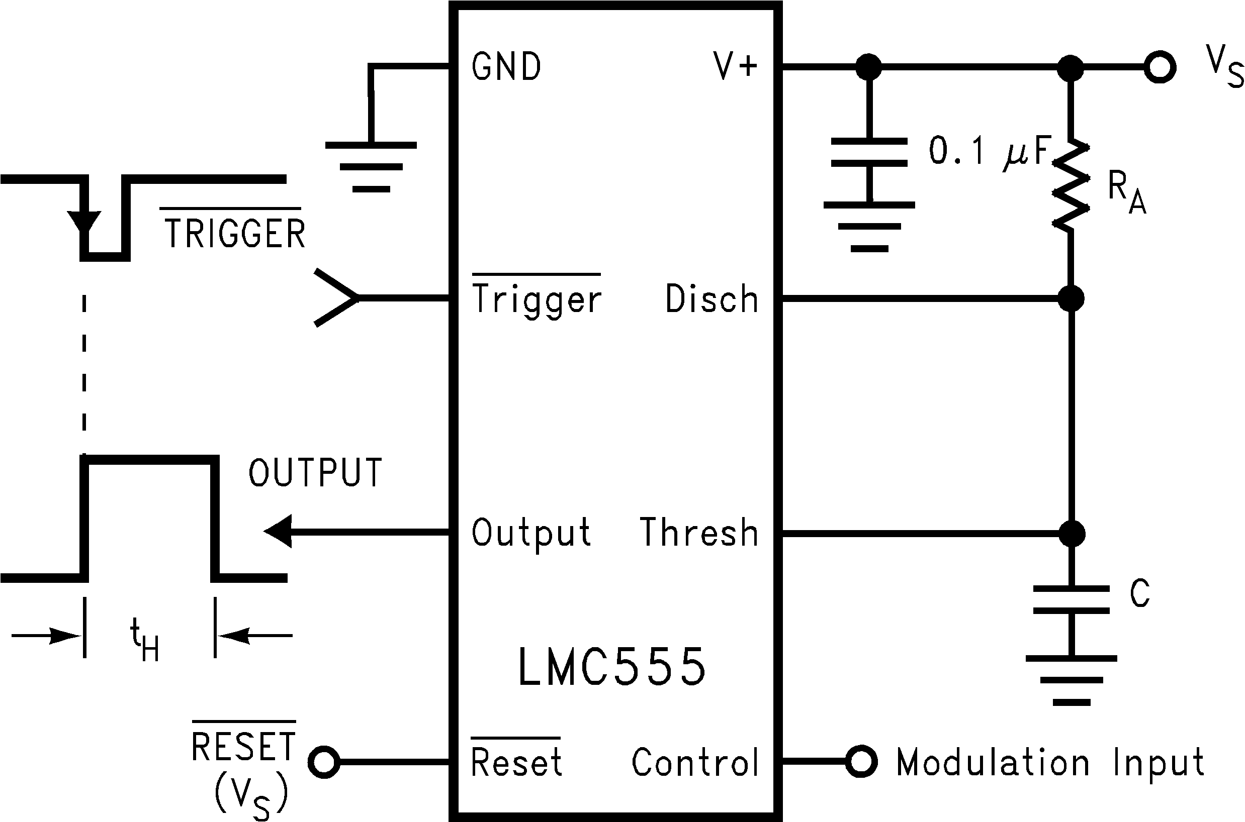
The LMC555 device is a CMOS version of the industry standard 555 series general-purpose timers. In addition to the standard SOIC, VSSSOP, and PDIP packages, the LMC555 is also available in a chip-sized, 8-bump DSBGA package using TI's DSBGA package technology. The LMC555 offers the same capability of generating accurate time delays and frequencies as the LM555, but with much lower power dissipation and supply current spikes. When operated as a one-shot, the time delay is precisely controlled by a single external resistor and capacitor. In astable mode, the oscillation frequency and duty cycle are accurately set by two external resistors and one capacitor. TI's LMCMOS process extends both the frequency range and the low supply capability.
| PART NUMBER | PACKAGE(1) | PACKAGE SIZE(2) |
|---|---|---|
| LMC555 | D (SOIC, 8) | 4.9mm × 6mm |
| DGK (VSSOP, 8) | 3mm × 4.9mm | |
| P (PDIP, 8) | 9.81mm × 9.43mm | |
| YBF (DSBGA, 8) | 1.75mm × 1.75mm |
 Pulse Width Modulator
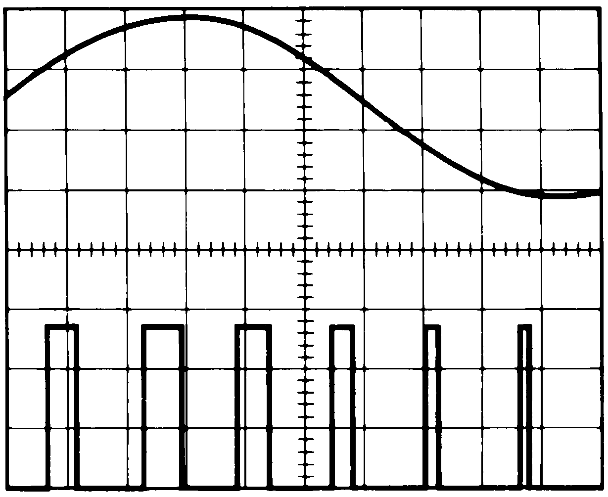
 Pulse Width Modulator Waveform:
 Top Waveform—Modulation
Bottom Waveform—Output Voltage