SNAS558N January   2000  – March 2024 LMC555

PRODUCTION DATA  

  1.   1
  2. Features
  3. Applications
  4. Description
  5. Pin Configuration and Functions
  6. Specifications
    1. 5.1 Absolute Maximum Ratings
    2. 5.2 ESD Ratings
    3. 5.3 Recommended Operating Conditions
    4. 5.4 Thermal Information
    5. 5.5 Electrical Characteristics
    6. 5.6 Switching Characteristics
  7. Parameter Measurement Information
  8. Detailed Description
    1. 7.1 Overview
    2. 7.2 Functional Block Diagram
    3. 7.3 Feature Description
      1. 7.3.1 Low-Power Dissipation
      2. 7.3.2 Various Packages and Compatibility
      3. 7.3.3 Operates in Both Astable and Monostable Mode
    4. 7.4 Device Functional Modes
      1. 7.4.1 Monostable Operation
      2. 7.4.2 Astable Operation
  9. Application and Implementation
    1. 8.1 Application Information
    2. 8.2 Typical Applications
      1. 8.2.1 Flash LED in Monostable Mode
        1. 8.2.1.1 Design Requirements
        2. 8.2.1.2 Detailed Design Procedure
        3. 8.2.1.3 Application Curve
      2. 8.2.2 Frequency Divider
        1. 8.2.2.1 Design Requirements
        2. 8.2.2.2 Application Curve
      3. 8.2.3 Pulse Width Modulator
        1. 8.2.3.1 Design Requirements
        2. 8.2.3.2 Application Curve
      4. 8.2.4 Pulse Position Modulator
        1. 8.2.4.1 Design Requirements
        2. 8.2.4.2 Application Curve
      5. 8.2.5 50% Duty Cycle Oscillator
        1. 8.2.5.1 Design Requirements
    3. 8.3 Power Supply Recommendations
    4. 8.4 Layout
      1. 8.4.1 Layout Guidelines
      2. 8.4.2 Layout Example
  10. Device and Documentation Support
    1. 9.1 Receiving Notification of Documentation Updates
    2. 9.2 Support Resources
    3. 9.3 Trademarks
    4. 9.4 Electrostatic Discharge Caution
    5. 9.5 Glossary
  11. 10Revision History
  12. 11Mechanical, Packaging, and Orderable Information

Package Options

Refer to the PDF data sheet for device specific package drawings

Mechanical Data (Package|Pins)
  • D|8
  • P|8
  • YPB|8
  • DGK|8
Thermal pad, mechanical data (Package|Pins)
Orderable Information

Application Curve

The data shown in Figure 8-2 were collected with the circuit used in the typical applications section. The LMC555 was configured in the monostable mode with a time delay of 5.17 s. The waveforms correspond to:

  • Top Waveform (Blue) – Capacitor voltage
  • Middle Waveform (Purple) – TRIGGER
  • Bottom Waveform (Green) – OUTPUT

As the TRIGGER pin pulses low, the capacitor voltage starts charging and the output goes high. The output goes low as soon as the capacitor voltage reaches 2/3 of the supply voltage, which is the time delay set by the R and C value. For this example, the time delay is 5.17 seconds.
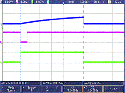
GUID-F92B198F-BA9A-4525-834C-AB87CD8EB610-low.gifFigure 8-2 TRIGGER, Capacitor Voltage, and OUTPUT Waveforms in Monostable Mode