SNOSD37B march 2017 – april 2023 LMG1205
PRODUCTION DATA
- 1 Features
- 2 Applications
- 3 Description
- 4 Revision History
- 5 Pin Configuration and Functions
- 6 Specifications
- 7 Detailed Description
- 8 Application and Implementation
- 9 Power Supply Recommendations
- 10Layout
- 11Device and Documentation Support
Package Options
Mechanical Data (Package|Pins)
- YFX|12
Thermal pad, mechanical data (Package|Pins)
Orderable Information
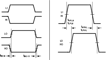
6.6 Switching Characteristics
over operating free-air temperature range (unless otherwise noted)
| PARAMETER | TEST CONDITIONS | MIN | TYP | MAX | UNIT | ||
|---|---|---|---|---|---|---|---|
| tLPHL | LO turnoff propagation delay | LI falling to LOL falling | TJ = 25°C | 33.5 | ns | ||
| TJ = –40°C to 125°C | 50 | ||||||
| tLPLH | LO turnon propagation delay | LI rising to LOH rising | TJ = 25°C | 35 | ns | ||
| TJ = –40°C to 125°C | 50 | ||||||
| tHPHL | HO turnoff propagation delay | HI falling to HOL falling | TJ = 25°C | 33.5 | ns | ||
| TJ = –40°C to 125°C | 50 | ||||||
| tHPLH | HO turnon propagation delay | HI rising to HOH rising | TJ = 25°C | 35 | ns | ||
| TJ = –40°C to 125°C | 50 | ||||||
| tMON | Delay matching LO on and HO off | TJ = 25°C | 1.5 | ns | |||
| TJ = –40°C to 125°C | 8 | ||||||
| tMOFF | Delay matching LO off and HO on | TJ = 25°C | 1.5 | ns | |||
| TJ = –40°C to 125°C | 8 | ||||||
| tHRC | HO rise time (0.5 V – 4.5 V) | CL = 1000 pF | 7 | ns | |||
| tLRC | LO rise time (0.5 V – 4.5 V) | CL = 1000 pF | 7 | ns | |||
| tHFC | HO fall time (0.5 V – 4.5 V) | CL = 1000 pF | 3.5 | ns | |||
| tLFC | LO fall time (0.5 V – 4.5 V) | CL = 1000 pF | 3.5 | ns | |||
| tPW | Minimum input pulse width that changes the output | 10 | ns | ||||
| tBS | Bootstrap diode reverse recovery time | IF = 100 mA, IR = 100 mA | 40 | ns | |||
(1) Parameters that show only a typical value are ensured by design and may not be tested in production.
 Figure 6-1 Timing Diagram