SNOSD37B march 2017 – april 2023 LMG1205
PRODUCTION DATA
- 1 Features
- 2 Applications
- 3 Description
- 4 Revision History
- 5 Pin Configuration and Functions
- 6 Specifications
- 7 Detailed Description
- 8 Application and Implementation
- 9 Power Supply Recommendations
- 10Layout
- 11Device and Documentation Support
Package Options
Mechanical Data (Package|Pins)
- YFX|12
Thermal pad, mechanical data (Package|Pins)
Orderable Information
8.2.2.1 VDD Bypass Capacitor
The VDD bypass capacitor provides the gate charge for the low-side and high-side transistors and to absorb the reverse recovery charge of the bootstrap diode. The required bypass capacitance can be calculated with Equation 1.
Equation 1. 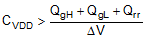
where
- QgH and QgL are gate charge of the high-side and low-side transistors, respectively
- Qrr is the reverse recovery charge of the bootstrap diode, which is typically around 4nC
- ΔV is the maximum allowable voltage drop across the bypass capacitor
TI recommends a 0.1–µF or larger value, good-quality ceramic capacitor. The bypass capacitor must be placed as close as possible to the device pins to minimize the parasitic inductance.