SNOSD37B march   2017  – april 2023 LMG1205

PRODUCTION DATA  

  1. Features
  2. Applications
  3. Description
  4. Revision History
  5. Pin Configuration and Functions
  6. Specifications
    1. 6.1 Absolute Maximum Ratings
    2. 6.2 ESD Ratings
    3. 6.3 Recommended Operating Conditions
    4. 6.4 Thermal Information
    5. 6.5 Electrical Characteristics
    6. 6.6 Switching Characteristics
    7. 6.7 Typical Characteristics
  7. Detailed Description
    1. 7.1 Overview
    2. 7.2 Functional Block Diagram
    3. 7.3 Feature Description
      1. 7.3.1 Input and Output
      2. 7.3.2 Start-up and UVLO
      3. 7.3.3 HS Negative Voltage and Bootstrap Supply Voltage Clamping
      4. 7.3.4 Level Shift
    4. 7.4 Device Functional Modes
  8. Application and Implementation
    1. 8.1 Application Information
    2. 8.2 Typical Application
      1. 8.2.1 Design Requirements
      2. 8.2.2 Detailed Design Procedure
        1. 8.2.2.1 VDD Bypass Capacitor
        2. 8.2.2.2 Bootstrap Capacitor
        3. 8.2.2.3 Power Dissipation
      3. 8.2.3 Application Curves
  9. Power Supply Recommendations
  10. 10Layout
    1. 10.1 Layout Guidelines
    2. 10.2 Layout Examples
  11. 11Device and Documentation Support
    1. 11.1 Device Support
      1. 11.1.1 Third-Party Products Disclaimer
    2. 11.2 Documentation Support
      1. 11.2.1 Related Documentation
    3. 11.3 Receiving Notification of Documentation Updates
    4. 11.4 Support Resources
    5. 11.5 Trademarks
    6. 11.6 Electrostatic Discharge Caution
    7. 11.7 Glossary
      1.      Mechanical, Packaging, and Orderable Information

Package Options

Mechanical Data (Package|Pins)
Thermal pad, mechanical data (Package|Pins)
Orderable Information

Typical Application

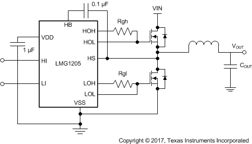
The circuit in Figure 8-1 shows a synchronous buck converter to evaluate LMG1205. Detailed synchronous buck converter specifications are listed in Section 8.2.1. Optimization of he power loop (loop impedance from VIN capacitor to PGND) is critical to the performance of the design. Having a high power loop inductance causes significant ringing in the SW node and also causes an associated power loss. For more information, please refer to Section 11.2.1.
GUID-7017698C-A054-4512-9B41-7FF884BC77A2-low.gifFigure 8-1 Application Circuit