SNOSD12D November   2018  – January 2019 LMG1210

PRODUCTION DATA.  

  1. Features
  2. Applications
  3. Description
    1.     Device Images
      1.      Simplified Typical Application
  4. Revision History
  5. Pin Configuration and Functions
    1.     Pin Functions
  6. Specifications
    1. 6.1 Absolute Maximum Ratings
    2. 6.2 ESD Ratings
    3. 6.3 Recommended Operating Conditions
    4. 6.4 Thermal Information
    5. 6.5 Electrical Characteristics
    6. 6.6 Switching Characteristics
    7. 6.7 Typical Characteristics
    8. 6.8 Timing Diagrams
  7. Detailed Description
    1. 7.1 Overview
    2. 7.2 Functional Block Diagram
    3. 7.3 Feature Description
      1. 7.3.1 Bootstrap Diode Operation
      2. 7.3.2 LDO Operation
      3. 7.3.3 Dead Time Selection
      4. 7.3.4 Overtemperature Protection
      5. 7.3.5 High-Performance Level Shifter
      6. 7.3.6 Negative HS Voltage Handling
    4. 7.4 Device Functional Modes
  8. Application and Implementation
    1. 8.1 Application Information
    2. 8.2 Typical Application
      1. 8.2.1 Design Requirements
      2. 8.2.2 Detailed Design Procedure
        1. 8.2.2.1 Bypass Capacitor
        2. 8.2.2.2 Bootstrap Diode Selection
        3. 8.2.2.3 Handling Ground Bounce
        4. 8.2.2.4 Independent Input Mode
        5. 8.2.2.5 Computing Power Dissipation
      3. 8.2.3 Application Curves
    3. 8.3 Do's and Don'ts
  9. Power Supply Recommendations
  10. 10Layout
    1. 10.1 Layout Guidelines
    2. 10.2 Layout Example
  11. 11Device and Documentation Support
    1. 11.1 Documentation Support
      1. 11.1.1 Related Documentation
    2. 11.2 Receiving Notification of Documentation Updates
    3. 11.3 Community Resources
    4. 11.4 Trademarks
    5. 11.5 Electrostatic Discharge Caution
    6. 11.6 Glossary
  12. 12Mechanical, Packaging, and Orderable Information

Package Options

Mechanical Data (Package|Pins)
  • RVR|19
Thermal pad, mechanical data (Package|Pins)
Orderable Information

Application Curves

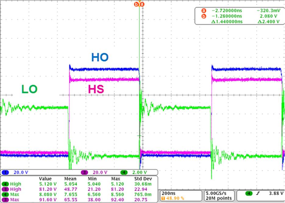
LMG1210 new-waveform-04-snvu572.jpgFigure 19. 1-MHz, 80-V Operation
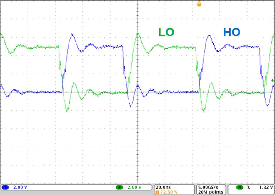
LMG1210 new-waveform-05-snvu572.jpgFigure 20. 10-MHz Operation, No Bus Voltage