SNLS568D March   2017  – May 2020 LMH1228

PRODUCTION DATA.  

  1. Features
  2. Applications
  3. Description
    1.     Simplified Block Diagram
  4. Revision History
  5. Pin Configuration and Functions
    1.     Pin Functions
  6. Specifications
    1. 6.1 Absolute Maximum Ratings
    2. 6.2 ESD Ratings
    3. 6.3 Recommended Operating Conditions
    4. 6.4 Thermal Information
    5. 6.5 Electrical Characteristics
    6. 6.6 Recommended SMBus Interface Timing Specifications
    7. 6.7 Serial Parallel Interface (SPI) Timing Specifications
    8. 6.8 Typical Characteristics
  7. Detailed Description
    1. 7.1 Overview
    2. 7.2 Functional Block Diagram
    3. 7.3 Feature Description
      1. 7.3.1 4-Level Input Pins and Thresholds
      2. 7.3.2 OUT0_SEL and SDI_OUT2_SEL Control
      3. 7.3.3 Input Signal Detect
      4. 7.3.4 Continuous Time Linear Equalizer (CTLE)
      5. 7.3.5 Clock and Data (CDR) Recovery
      6. 7.3.6 Internal Eye Opening Monitor (EOM)
      7. 7.3.7 Output Function Control
      8. 7.3.8 Output Driver Control
        1. 7.3.8.1 Line-Side Output Cable Driver (SDI_OUT1+, SDI_OUT2+)
          1. 7.3.8.1.1 Output Amplitude (VOD)
          2. 7.3.8.1.2 Output Pre-Emphasis
          3. 7.3.8.1.3 Output Slew Rate
          4. 7.3.8.1.4 Output Polarity Inversion
        2. 7.3.8.2 Host-Side 100-Ω Output Driver (OUT0±)
      9. 7.3.9 Status Indicators and Interrupts
        1. 7.3.9.1 LOCK_N (Lock Indicator)
        2. 7.3.9.2 SD_N (Signal Detect)
        3. 7.3.9.3 INT_N (Interrupt)
    4. 7.4 Device Functional Modes
      1. 7.4.1 System Management Bus (SMBus) Mode
        1. 7.4.1.1 SMBus Read and Write Transaction
          1. 7.4.1.1.1 SMBus Write Operation Format
          2. 7.4.1.1.2 SMBus Read Operation Format
      2. 7.4.2 Serial Peripheral Interface (SPI) Mode
        1. 7.4.2.1 SPI Read and Write Transactions
        2. 7.4.2.2 SPI Write Transaction Format
        3. 7.4.2.3 SPI Read Transaction Format
        4. 7.4.2.4 SPI Daisy Chain
    5. 7.5 Register Maps
  8. Application and Implementation
    1. 8.1 Application Information
      1. 8.1.1 SMPTE Requirements and Specifications
      2. 8.1.2 Low-Power Optimization
      3. 8.1.3 Optimized Loop Bandwidth Settings for Arria 10 FPGA Applications
    2. 8.2 Typical Applications
      1. 8.2.1 Dual Cable Driver
        1. 8.2.1.1 Design Requirements
        2. 8.2.1.2 Detailed Design Procedure
        3. 8.2.1.3 Application Curves
      2. 8.2.2 Distribution Amplifier
        1. 8.2.2.1 Design Requirements
        2. 8.2.2.2 Detailed Design Procedure
        3. 8.2.2.3 Application Curves
  9. Power Supply Recommendations
  10. 10Layout
    1. 10.1 Layout Guidelines
      1. 10.1.1 Board Stack-Up and Ground References
      2. 10.1.2 High-Speed PCB Trace Routing and Coupling
        1. 10.1.2.1 SDI_OUT1± and SDI_OUT2±:
        2. 10.1.2.2 IN0± and OUT0±:
      3. 10.1.3 Anti-Pads
      4. 10.1.4 BNC Connector Layout and Routing
      5. 10.1.5 Power Supply and Ground Connections
      6. 10.1.6 Footprint Recommendations
    2. 10.2 Layout Example
  11. 11Device and Documentation Support
    1. 11.1 Documentation Support
      1. 11.1.1 Related Documentation
    2. 11.2 Receiving Notification of Documentation Updates
    3. 11.3 Support Resources
    4. 11.4 Trademarks
    5. 11.5 Electrostatic Discharge Caution
    6. 11.6 Export Control Notice
    7. 11.7 Glossary
  12. 12Mechanical, Packaging, and Orderable Information
    1. 12.1 Package Option Addendum
      1. 12.1.1 Packaging Information
      2. 12.1.2 Tape and Reel Information

Package Options

Mechanical Data (Package|Pins)
Thermal pad, mechanical data (Package|Pins)
Orderable Information

Description

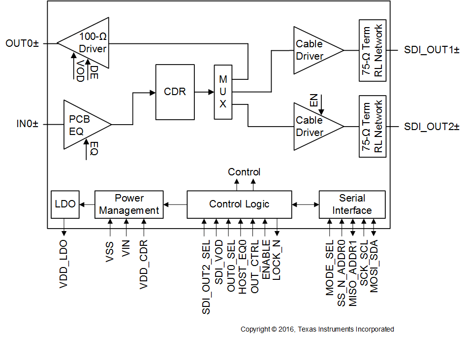
LMH1228 device is a 12G UHD-SDI low power dual output cable driver with integrated reclocker. It supports SMPTE video rates up to 11.88 Gbps, enabling UHD video for 4K/8K applications. With a wide range clock-and-data recovery (CDR) circuit, the on-chip reclocker automatically detects and locks to all SMPTE video rates up to 11.88 Gbps. The additional reclocked 100-Ω driver output on the host-side can be used for monitoring or signal distribution purposes.

The on-chip reclocker attenuates high-frequency jitter and fully regenerates the data using a clean, low-jitter clock. The reclocker has a built-in loop filter and does not require any input reference clock. The LMH1228 also has an internal eye opening monitor and a programmable pin for CDR lock indication, input signal detect, or hardware interrupts to support system diagnostics and board bring-up.

The LMH1228 is powered from a single 2.5-V supply. It is offered in a small footprint 5 mm × 5 mm 32-pin WQFN package. The LMH1228 is pin compatible with the LMH1208 (12G Dual Cable Driver).

Device Information(1)

PART NUMBER PACKAGE BODY SIZE (NOM)
LMH1228 WQFN (32) 5.00 mm × 5.00 mm
  1. For all available packages, see the orderable addendum at the end of the data sheet.

Simplified Block Diagram
LMH1228 front_page_block_diagram_lmh1228_snls575.gif