SNLS568D March   2017  – May 2020 LMH1228

PRODUCTION DATA.  

  1. Features
  2. Applications
  3. Description
    1.     Simplified Block Diagram
  4. Revision History
  5. Pin Configuration and Functions
    1.     Pin Functions
  6. Specifications
    1. 6.1 Absolute Maximum Ratings
    2. 6.2 ESD Ratings
    3. 6.3 Recommended Operating Conditions
    4. 6.4 Thermal Information
    5. 6.5 Electrical Characteristics
    6. 6.6 Recommended SMBus Interface Timing Specifications
    7. 6.7 Serial Parallel Interface (SPI) Timing Specifications
    8. 6.8 Typical Characteristics
  7. Detailed Description
    1. 7.1 Overview
    2. 7.2 Functional Block Diagram
    3. 7.3 Feature Description
      1. 7.3.1 4-Level Input Pins and Thresholds
      2. 7.3.2 OUT0_SEL and SDI_OUT2_SEL Control
      3. 7.3.3 Input Signal Detect
      4. 7.3.4 Continuous Time Linear Equalizer (CTLE)
      5. 7.3.5 Clock and Data (CDR) Recovery
      6. 7.3.6 Internal Eye Opening Monitor (EOM)
      7. 7.3.7 Output Function Control
      8. 7.3.8 Output Driver Control
        1. 7.3.8.1 Line-Side Output Cable Driver (SDI_OUT1+, SDI_OUT2+)
          1. 7.3.8.1.1 Output Amplitude (VOD)
          2. 7.3.8.1.2 Output Pre-Emphasis
          3. 7.3.8.1.3 Output Slew Rate
          4. 7.3.8.1.4 Output Polarity Inversion
        2. 7.3.8.2 Host-Side 100-Ω Output Driver (OUT0±)
      9. 7.3.9 Status Indicators and Interrupts
        1. 7.3.9.1 LOCK_N (Lock Indicator)
        2. 7.3.9.2 SD_N (Signal Detect)
        3. 7.3.9.3 INT_N (Interrupt)
    4. 7.4 Device Functional Modes
      1. 7.4.1 System Management Bus (SMBus) Mode
        1. 7.4.1.1 SMBus Read and Write Transaction
          1. 7.4.1.1.1 SMBus Write Operation Format
          2. 7.4.1.1.2 SMBus Read Operation Format
      2. 7.4.2 Serial Peripheral Interface (SPI) Mode
        1. 7.4.2.1 SPI Read and Write Transactions
        2. 7.4.2.2 SPI Write Transaction Format
        3. 7.4.2.3 SPI Read Transaction Format
        4. 7.4.2.4 SPI Daisy Chain
    5. 7.5 Register Maps
  8. Application and Implementation
    1. 8.1 Application Information
      1. 8.1.1 SMPTE Requirements and Specifications
      2. 8.1.2 Low-Power Optimization
      3. 8.1.3 Optimized Loop Bandwidth Settings for Arria 10 FPGA Applications
    2. 8.2 Typical Applications
      1. 8.2.1 Dual Cable Driver
        1. 8.2.1.1 Design Requirements
        2. 8.2.1.2 Detailed Design Procedure
        3. 8.2.1.3 Application Curves
      2. 8.2.2 Distribution Amplifier
        1. 8.2.2.1 Design Requirements
        2. 8.2.2.2 Detailed Design Procedure
        3. 8.2.2.3 Application Curves
  9. Power Supply Recommendations
  10. 10Layout
    1. 10.1 Layout Guidelines
      1. 10.1.1 Board Stack-Up and Ground References
      2. 10.1.2 High-Speed PCB Trace Routing and Coupling
        1. 10.1.2.1 SDI_OUT1± and SDI_OUT2±:
        2. 10.1.2.2 IN0± and OUT0±:
      3. 10.1.3 Anti-Pads
      4. 10.1.4 BNC Connector Layout and Routing
      5. 10.1.5 Power Supply and Ground Connections
      6. 10.1.6 Footprint Recommendations
    2. 10.2 Layout Example
  11. 11Device and Documentation Support
    1. 11.1 Documentation Support
      1. 11.1.1 Related Documentation
    2. 11.2 Receiving Notification of Documentation Updates
    3. 11.3 Support Resources
    4. 11.4 Trademarks
    5. 11.5 Electrostatic Discharge Caution
    6. 11.6 Export Control Notice
    7. 11.7 Glossary
  12. 12Mechanical, Packaging, and Orderable Information
    1. 12.1 Package Option Addendum
      1. 12.1.1 Packaging Information
      2. 12.1.2 Tape and Reel Information

Package Options

Mechanical Data (Package|Pins)
Thermal pad, mechanical data (Package|Pins)
Orderable Information

Dual Cable Driver

The LMH1228 can be configured as a dual cable driver to route the same SDI output signal to multiple receivers. In this configuration, the LMH1228 adaptively equalizes 100-Ω SDI input data at IN0 and uses the dual cable drivers at SDI_OUT1 and SDI_OUT2 to drive out the SDI signal.

Figure 21 shows a typical application of an LMH1228 as a dual cable driver output. In this example, the LMH1219 Cable EQ with Integrated Reclocker provides an SDI input to the SDI FPGA. The FPGA then sends post-processed SDI data to the IN0 of the LMH1228, which drives the data on cable driver outputs SDI_OUT1 and SDI_OUT2.
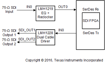
LMH1228 typical_application_dual_cable_driver_snls575.gifFigure 21. LMH1228 Dual Cable Driver Application