SBOS695A August 2014 – December 2014 LMH3401
PRODUCTION DATA.
- 1 Features
- 2 Applications
- 3 Description
- 4 Revision History
- 5 Device Comparison Table
- 6 Pin Configuration and Functions
- 7 Specifications
- 8 Parameter Measurement Information
- 9 Detailed Description
-
10Application and Implementation
- 10.1 Application Information
- 10.2 Typical Application
- 10.3 Do's and Don'ts
- 11Power-Supply Recommendations
- 12Layout
- 13Device and Documentation Support
- 14Mechanical, Packaging, and Orderable Information
Package Options
Mechanical Data (Package|Pins)
- RMS|14
Thermal pad, mechanical data (Package|Pins)
Orderable Information
1 Features
- Excellent Single-Ended to Differential Conversion Performance from DC to 2 GHz
- 7-GHz, –3-dB Bandwidth
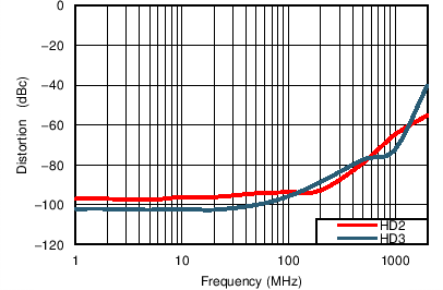
- Excellent HD2 and HD3 to 2 GHz:
- –96 (HD2), –102 (HD3) at 10 MHz
- –79 (HD2), –77 (HD3) at 500 MHz
- –64 (HD2), –72 (HD3) at 1 GHz
- –55 (HD2), –40 (HD3) at 2 GHz
- Best in Class OIP3 Performance to 2 GHz:
- 45 dBm at 200 MHz
- 33 dBm at 1 GHz
- 24 dBm at 2 GHz
- Fixed Single-Ended to Differential Voltage Gain: 16 dB
- Noise Figure: 9 dB at 200 MHz (RS = 50 Ω)
- Slew Rate: 18,000 V/µs
- Supports Single-Supply or Split-Supply Operation
- Powered-Down Feature
- Supply Current: 55 mA
2 Applications
- GSPS ADC Drivers
- ADC Drivers for High-Speed Data Acquisition
- ADC Driver for 1-GBPS Ethernet over Microwave
- DAC Buffers
- Wideband Gain Stages
- Single-Ended to Differential Conversions
- Level Shifters
3 Description
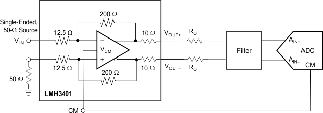
The LMH3401 is a very high-performance, differential amplifier optimized for radio frequency (RF), intermediate frequency (IF), or high-speed, time-domain applications. This device is ideal for dc- or ac-coupled applications that require a single-ended to differential conversion when driving an analog-to-digital converter (ADC). The LMH3401 generates very low levels of second-order and third-order distortion when operating in single-ended-input to differential-output or differential-input to differential-output mode.
The on-chip resistors simplify printed circuit board (PCB) implementation and provide the highest performance over the usable bandwidth of 2 GHz. This performance makes the LMH3401 ideal for applications such as test and measurement, broadband communications, and high-speed data acquisition. A common-mode reference input pin is provided to align the amplifier output common-mode with the ADC input requirements. Use this device with power supplies between 3.3 V and 5.0 V; dual-supply operation is supported when required by the application.
This level of performance is achieved at a very low power level of 275 mW when a 5.0-V supply is used. A power-down feature is also available for power savings. The LMH3401 is fabricated in Texas Instruments' advanced complementary BiCMOS process and is available in a space-saving, 14-lead UQFN package with a specified operating temperature range of –40°C to 85°C.
Device Information(1)
| PART NUMBER | PACKAGE | BODY SIZE (NOM) |
|---|---|---|
| LMH3401 | UQFN (14) | 2.50 mm × 2.50 mm |
- For all available packages, see the orderable addendum at the end of the datasheet.