SBOS695A August 2014 – December 2014 LMH3401
PRODUCTION DATA.
- 1 Features
- 2 Applications
- 3 Description
- 4 Revision History
- 5 Device Comparison Table
- 6 Pin Configuration and Functions
- 7 Specifications
- 8 Parameter Measurement Information
- 9 Detailed Description
-
10Application and Implementation
- 10.1 Application Information
- 10.2 Typical Application
- 10.3 Do's and Don'ts
- 11Power-Supply Recommendations
- 12Layout
- 13Device and Documentation Support
- 14Mechanical, Packaging, and Orderable Information
Package Options
Mechanical Data (Package|Pins)
- RMS|14
Thermal pad, mechanical data (Package|Pins)
Orderable Information
6 Pin Configuration and Functions
RMS Package
UQFN-14
(Top View)
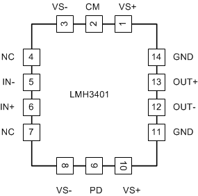
Pin Functions
| PIN | I/O | DESCRIPTION | |
|---|---|---|---|
| NAME | NO. | ||
| CM | 2 | I | Output common-mode voltage control input pin |
| GND | 11, 14 | P | Ground. This ground does not impact the signal path, this pin is the reference for the digital input pin (PD). |
| IN– | 5 | I | Inverting input pin |
| IN+ | 6 | I | Noninverting input pin |
| NC | 4, 7 | — | No internal connection |
| OUT– | 12 | O | Inverting output pin |
| OUT+ | 13 | O | Noninverting output pin |
| PD | 9 | I | Power down. High (> GND + 1.2 V) = low-power (sleep) mode. Low (< GND + 0.9 V) = active. |
| VS– | 3, 8 | P | Power-supply pins, negative rail |
| VS+ | 1, 10 | P | Power-supply pins, positive rail |