SBOS695A August   2014  – December 2014 LMH3401

PRODUCTION DATA.  

  1. Features
  2. Applications
  3. Description
  4. Revision History
  5. Device Comparison Table
  6. Pin Configuration and Functions
  7. Specifications
    1. 7.1 Absolute Maximum Ratings
    2. 7.2 ESD Ratings
    3. 7.3 Recommended Operating Conditions
    4. 7.4 Thermal Information
    5. 7.5 Electrical Characteristics: VS = 5 V
    6. 7.6 Electrical Characteristics: VS = 3.3 V
    7. 7.7 Typical Characteristics
  8. Parameter Measurement Information
    1. 8.1  Output Reference Points
    2. 8.2  ATE Testing and DC Measurements
    3. 8.3  Frequency Response
    4. 8.4  S-Parameters
    5. 8.5  Frequency Response with Capacitive Load
    6. 8.6  Distortion
    7. 8.7  Noise Figure
    8. 8.8  Pulse Response, Slew Rate, Overdrive Recovery
    9. 8.9  Power Down
    10. 8.10 VCM Frequency Response
    11. 8.11 Test Schematics
  9. Detailed Description
    1. 9.1 Overview
    2. 9.2 Functional Block Diagram
    3. 9.3 Feature Description
      1. 9.3.1 Fully-Differential Amplifier
      2. 9.3.2 Single-Ended to Differential Signals
        1. 9.3.2.1 Resistor Design Equations for Single-to-Differential Applications
        2. 9.3.2.2 Input Impedance Calculations
      3. 9.3.3 Differential to Differential Signals
      4. 9.3.4 Output Common-Mode Voltage
    4. 9.4 Device Functional Modes
      1. 9.4.1 Operation with a Split Supply
      2. 9.4.2 Operation with a Single Supply
  10. 10Application and Implementation
    1. 10.1 Application Information
      1. 10.1.1 Input and Output Headroom Considerations
      2. 10.1.2 Noise Analysis
      3. 10.1.3 Thermal Considerations
    2. 10.2 Typical Application
      1. 10.2.1 Design Requirements
      2. 10.2.2 Detailed Design Procedure
        1. 10.2.2.1 Driving Matched Loads
        2. 10.2.2.2 Driving Capacitive Loads
        3. 10.2.2.3 Driving ADCs
          1. 10.2.2.3.1 SNR Considerations
          2. 10.2.2.3.2 SFDR Considerations
          3. 10.2.2.3.3 ADC Input Common-Mode Voltage Considerations—AC-Coupled Input
          4. 10.2.2.3.4 ADC Input Common-Mode Voltage Considerations—DC-Coupled Input
        4. 10.2.2.4 GSPS ADC Driver
        5. 10.2.2.5 Common-Mode Voltage Correction
        6. 10.2.2.6 Active Balun
        7. 10.2.2.7 Application Curves
    3. 10.3 Do's and Don'ts
      1. 10.3.1 Do:
      2. 10.3.2 Don't:
  11. 11Power-Supply Recommendations
    1. 11.1 Supply Voltage
    2. 11.2 Single Supply
    3. 11.3 Split Supply
    4. 11.4 Supply Decoupling
  12. 12Layout
    1. 12.1 Layout Guidelines
    2. 12.2 Layout Example
  13. 13Device and Documentation Support
    1. 13.1 Device Support
      1. 13.1.1 Device Nomenclature
    2. 13.2 Documentation Support
      1. 13.2.1 Related Documentation
    3. 13.3 Trademarks
    4. 13.4 Electrostatic Discharge Caution
    5. 13.5 Glossary
  14. 14Mechanical, Packaging, and Orderable Information

Package Options

Mechanical Data (Package|Pins)
Thermal pad, mechanical data (Package|Pins)
Orderable Information

13 Device and Documentation Support

13.1 Device Support

13.1.1 Device Nomenclature

device_markings_bos695.gif
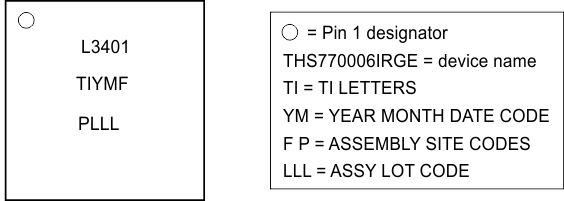
Figure 73. Device Marking Information

13.2 Documentation Support

13.2.1 Related Documentation

For related documentation see the following:

  • THS4541 Data Sheet, SLOS375
  • ADS12D1800RF Data Sheet, SNAS518
  • ADS5424 Data Sheet, SLWS157
  • ADS5485 Data Sheet, SLAS610
  • ADS6149 Data Sheet, SLWS211
  • ADS4149 Data Sheet, SBAS483
  • LMH3401EVM Evaluation Module, SBOU124
  • AN-2188 Between the Amplifier and the ADC: Managing Filter Loss in Communications Systems, SNOA567
  • AN-2235 Circuit Board Design for LMH6517/21/22 and Other High-Speed IF/RF Feedback Amplifiers, SNOA869

13.3 Trademarks

Marki is a trademark of Marki Microwave, Inc.

Rohde & Schwarz is a registered trademark of Rohde & Schwarz.

All other trademarks are the property of their respective owners.

13.4 Electrostatic Discharge Caution

esds-image

This integrated circuit can be damaged by ESD. Texas Instruments recommends that all integrated circuits be handled with appropriate precautions. Failure to observe proper handling and installation procedures can cause damage.

ESD damage can range from subtle performance degradation to complete device failure. Precision integrated circuits may be more susceptible to damage because very small parametric changes could cause the device not to meet its published specifications.

13.5 Glossary

SLYZ022TI Glossary.

This glossary lists and explains terms, acronyms, and definitions.