SBOS695A August 2014 – December 2014 LMH3401
PRODUCTION DATA.
- 1 Features
- 2 Applications
- 3 Description
- 4 Revision History
- 5 Device Comparison Table
- 6 Pin Configuration and Functions
- 7 Specifications
- 8 Parameter Measurement Information
- 9 Detailed Description
-
10Application and Implementation
- 10.1 Application Information
- 10.2 Typical Application
- 10.3 Do's and Don'ts
- 11Power-Supply Recommendations
- 12Layout
- 13Device and Documentation Support
- 14Mechanical, Packaging, and Orderable Information
Package Options
Mechanical Data (Package|Pins)
- RMS|14
Thermal pad, mechanical data (Package|Pins)
Orderable Information
10 Application and Implementation
NOTE
Information in the following applications sections is not part of the TI component specification, and TI does not warrant its accuracy or completeness. TI’s customers are responsible for determining suitability of components for their purposes. Customers should validate and test their design implementation to confirm system functionality.
10.1 Application Information
10.1.1 Input and Output Headroom Considerations
The starting point for most designs is to assign an output common-mode voltage. For ac-coupled signal paths, this starting point is often the default mid-supply voltage to retain the most available output swing around the output operating point, which is centered with Vcm equal to the mid-supply point. For dc-coupled designs, set this voltage while considering the required minimum headroom to the supplies listed in the Electrical Characteristics for VCM control. From that target output VCM, the next step is to verify that the desired output differential VPP stays within the supplies. For any desired differential output voltage (VOPP) check the maximum possible signal swing for each output pin. Make sure that each pin can swing to the voltage required by the application.
For instance, when driving the ADC12D1800RF with a 1.25-V common-mode and 0.8-VPP input swing, the maximum output swing is set by the negative-going signal from 1.25 V to 0.2 V. The negative swing of the signal is right at the edge of the output swing capability of the LMH3401. In order to set the output common-mode to an acceptable range, a negative power supply of at least –1 V is recommended. The ideal negative supply voltage is the ADC VCM – 2.5 V for the negative supply and the ADC VCM + 2.5 V for the input swing. In order to use the existing supply rails, deviating from the ideal voltage may be necessary.
With the output headroom confirmed, the input junctions must also stay within their operating range. Because the input range extends nearly to the negative supply voltage, input range limitations only appear when approaching the positive supply where a maximum 1.5-V headroom is required.
The input pins operate at voltages set by the external circuit design, the required output VOCM, and the input signal characteristics. The operating voltage of the input pins depends on the external circuit design. With a differential input, the input pins operate at a fixed input VICM, and the differential input signal does not influence this common-mode operating voltage.
AC-coupled differential input designs have a VICM equal to the output VOCM. DC-coupled differential input designs must check the voltage divider from the source VCM to the LMH3401 CM setting. That result solves to an input VICM within the specified range. If the source VCM can vary over some voltage range, the validation calculations must include this variation.
10.1.2 Noise Analysis
The first step in the output noise analysis is to reduce the application circuit to its simplest form with equal feedback and gain setting elements to ground (see Figure 58) with the FDA and resistor noise terms to be considered. For most single-ended input applications, the LMH3401 has RF = 200 Ω and RG = 12.5 Ω + 50 Ω. The noise equations show the benefit of active termination when using the LMH3401 for single-ended inputs. The LMH3401 internal resistors are not 50 Ω, as is the case with resistive termination. Thus, active termination gives a significant reduction in noise.
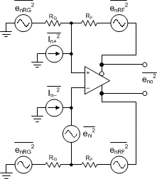 Figure 58. FDA Noise-Analysis Circuit
The noise powers are shown in Figure 58 for each term. When the RF and RG terms are matched on each side, the total differential output noise is the root sum of squares (RSS) of these separate terms. Using NG ≡ 1 + RF / RG, the total output noise is given by Equation 7. Each resistor noise term is a 4-kTR power.
The first term is simply the differential input spot noise times the noise gain. The second term is the input current noise terms times the feedback resistor (and because there are two terms, the power is two times one of the terms). The last term is the output noise resulting from both the RF and RG resistors, again times two, for the output noise power of each side added together. Using the exact values for a 50-Ω, matched, single-ended to differential gain, sweep with a fixed RF = 200 Ω and the intrinsic noise eni = 1.4 nV and In = 2.5 pA for the LMH3401, which gives an output spot noise from Equation 7. Then, dividing by the signal gain (AV) gives the input-referred, spot-noise voltage (ei). Note that for the LMH3401 the current noise is an insignificant noise contributor because of the low value of RF.
10.1.3 Thermal Considerations
The LMH3401 is packaged in a space-saving UQFN package that has a thermal coefficient (RθJA) of 101°C/W. Limit the total power dissipation in order to keep the device junction temperature below 150°C for instantaneous power and below 125°C for continuous power.
10.2 Typical Application
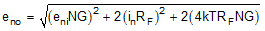
The LMH3401 is designed as a single-ended to differential conversion block with gain. The LMH3401 has no low-end frequency cutoff and has 7 GHz of bandwidth. The LMH3401 is a very attractive substitute for a balun transformer in many applications.
The resistors labeled RO serve to match the filter impedance the to 20-Ω amplifier output impedance. If no filter is used these resistors may not be required if the ADC is located very close to the LMH3401. If there is a transmission line between the LMH3401 and the ADC then the RO resistors must be sized to match the transmission line impedance. A typical application driving an ADC is shown in Figure 59.
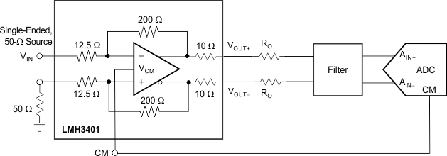 Figure 59. Single-Ended Input ADC Driver
10.2.1 Design Requirements
The main design requirements are to keep the amplifier input and output common-mode voltages compatible with the ADC requirements and the amplifier requirements. Using split power supplies may be required.
10.2.2 Detailed Design Procedure
10.2.2.1 Driving Matched Loads
The LMH3401 has on-chip output resistors, however for most load conditions additional resistance must be added to the output to match a desired load. Table 1 lists the matching resistors for some common load conditions.
Table 1. Load Component Values(1)
| LOAD (RL) | RO+ AND RO– FOR A MATCHED TERMINATION | TOTAL LOAD RESISTANCE AT AMPLIFIER OUTPUT | TERMINATION LOSS |
|---|---|---|---|
| 50Ω | 15 Ω | 100 Ω | 6 dB |
| 100 Ω | 40 Ω | 200 Ω | 6 dB |
| 200 Ω | 90 Ω | 400 Ω | 6 dB |
| 400 Ω | 190 Ω | 800 Ω | 6 dB |
| 1 kΩ | 490 Ω | 2000 Ω | 6 dB |
10.2.2.2 Driving Capacitive Loads
With high-speed signal paths, capacitive loading is highly detrimental to the signal path, as shown in Figure 60. Designers must make every effort to reduce parasitic loading on the amplifier output pins. The device on-chip resistors are included in order to isolate the parasitic capacitance associated with the package and the PCB pads that the device is soldered to. The LMH3401 is stable with most capacitive loads up to 10 pF; however, bandwidth suffers with capacitive loading on the output.
 Figure 60. Frequency Response with Capacitive Load
10.2.2.3 Driving ADCs
The LMH3401 is designed and optimized for the highest performance to drive differential input ADCs. Figure 61 shows a generic block diagram of the LMH3401 driving an ADC. The primary interface circuit between the amplifier and the ADC is usually a filter of some type for antialias purposes, and provides a means to bias the signal to the input common-mode voltage required by the ADC. Filters range from single-order real RC poles to higher-order LC filters, depending on the requirements of the application. Output resistors (RO) are shown on the amplifier outputs to isolate the amplifier from any capacitive loading presented by the filter.
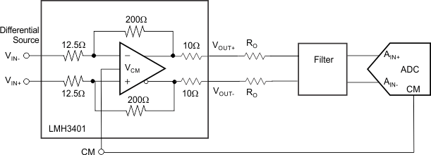 Figure 61. Differential ADC Driver Block Diagram
The key points to consider for implementation are the SNR, SFDR, and ADC input considerations, as described in this section. When the application circuit requires an input match, external resistors can be used such as shown in Figure 62.
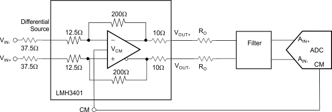 Figure 62. Using External Resistors for Matching a 100-Ω Source
10.2.2.3.1 SNR Considerations
The signal-to-noise ratio (SNR) of the amplifier and filter can be calculated from the amplitude of the signal and the bandwidth of the filter. The noise from the amplifier is band-limited by the filter with the equivalent brick-wall filter bandwidth. The amplifier and filter noise can be calculated using Equation 8:
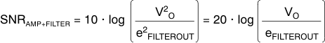
where
- eFILTEROUT = eNAMPOUT • √ENB,
- eNAMPOUT = the output noise density of the LMH3401 (3.4 nV/√Hz),
- ENB = the brick-wall equivalent noise bandwidth of the filter, and
- VO = the amplifier output signal.
For example, with a first-order (N = 1) band-pass or low-pass filter with a 30-MHz cutoff, the ENB is 1.57 • f–3dB = 1.57 • 30 MHz = 47.1 MHz. For second-order (N = 2) filters, the ENB is 1.22 • f–3dB. As the filter order increases, the ENB approaches f–3dB (N = 3 → ENB = 1.15 • f–3dB; N = 4 → ENB = 1.13 • f–3dB). Both VO and eFILTEROUT are in RMS voltages. For example, with a 2-VPP (0.707 VRMS) output signal and a 30-MHz first-order filter, the SNR of the amplifier and filter is 70.7 dB with eFILTEROUT = 3.4 nV/√Hz • √47.1 MHz = 23 μVRMS.
The SNR of the amplifier, filter, and ADC sum in RMS fashion, is as shown in Equation 9 (SNR values in dB):
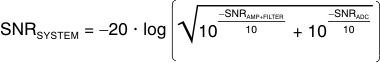
This formula shows that if the SNR of the amplifier and filter equals the SNR of the ADC, the combined SNR is
3 dB lower (worse). Thus, for minimal degradation (< 1 dB) on the ADC SNR, the SNR of the amplifier and filter must be ≥ 10 dB greater than the ADC SNR. The combined SNR calculated in this manner is usually accurate to within ±1 dB of the actual implementation.
10.2.2.3.2 SFDR Considerations
The SFDR of the amplifier is usually set by the second-order or third-order harmonic distortion for single-tone inputs, and by the second-order or third-order intermodulation distortion for two-tone inputs. Harmonics and second-order intermodulation distortion can be filtered to some degree, but third-order intermodulation spurs cannot be filtered. The ADC generates the same distortion products as the amplifier, but as a result of the sampling and clock feedthrough, additional spurs (not linearly related to the input signal) are included.
When the spurs from the amplifier and filter are known, each individual spur can be directly added to the same spur from the ADC, as shown in Equation 10, to estimate the combined spur (spur amplitudes in dBc):
This calculation assumes the spurs are in phase, but usually provides a good estimate of the final combined distortion.
For example, if the spur of the amplifier and filter equals the spur of the ADC, then the combined spur is 6 dB higher. To minimize the amplifier contribution (< 1 dB) to the overall system distortion, the spur from the amplifier and filter must be approximately 15 dB lower in amplitude than that of the converter. The combined spur calculated in this manner is usually accurate to within ±6 dB of the actual implementation; however, higher variations can be detected as a result of phase shift in the filter, especially in second-order harmonic performance.
This worst-case spur calculation assumes that the amplifier and filter spur of interest is in phase with the corresponding spur in the ADC, such that the two spur amplitudes can be added linearly. There are two phase-shift mechanisms that cause the measured distortion performance of the amplifier-ADC chain to deviate from the expected performance calculated using Equation 10: common-mode phase shift and differential phase shift.
Common-mode phase shift is the phase shift detected equally in both branches of the differential signal path including the filter. Common-mode phase shift nullifies the basic assumption that the amplifier, filter, and ADC spur sources are in phase. This phase shift can lead to better performance than predicted when the spurs become phase shifted, and there is the potential for cancellation when the phase shift reaches 180°. However, there is a significant challenge in designing an amplifier-ADC interface circuit to take advantage of a common-mode phase shift for cancellation: the phase characteristic of the ADC spur sources are unknown, thus the necessary phase shift in the filter and signal path for cancellation is also unknown.
Differential phase shift is the difference in the phase response between the two branches of the differential filter signal path. Differential phase shift in the filter as a result of mismatched components caused by nominal tolerance can severely degrade the even-order distortion of the amplifier-ADC chain. This effect has the same result as mismatched path lengths for the two differential traces, and causes more phase shift in one path than the other. Ideally, the phase response over frequency through the two sides of a differential signal path are identical, such that even-order harmonics remain optimally out of phase and cancel when the signal is taken differentially. However, if one side has more phase shift than the other, then the even-order harmonic cancellation is not as effective.
Single-order RC filters cause very little differential phase shift with nominal tolerances of 5% or less, but higher-order LC filters are very sensitive to component mismatch. For instance, a third-order Butterworth bandpass filter with a 100-MHz center frequency and a 20-MHz bandwidth shows as much as 20° of differential phase imbalance in a SPICE Monte Carlo analysis with 2% component tolerances. Therefore, while a prototype may work, production variance is unacceptable. In ac-coupled applications that require second- and higher-order filters between the LMH3401 and ADC, a transformer or balun is recommended at the ADC input to restore the phase balance. For dc-coupled applications where a transformer or balun at the ADC input cannot be used, using first- or second-order filters is recommended to minimize the effect of differential phase shift because of the component tolerance.
10.2.2.3.3 ADC Input Common-Mode Voltage Considerations—AC-Coupled Input
The input common-mode voltage range of the ADC must be respected for proper operation. In an ac-coupled application between the amplifier and the ADC, the input common-mode voltage bias of the ADC is accomplished in different ways depending on the ADC. Some ADCs use internal bias networks such that the analog inputs are automatically biased to the required input common-mode voltage if the inputs are ac-coupled with capacitors (or if the filter between the amplifier and ADC is a band-pass filter). Other ADCs supply their required input common-mode voltage from a reference voltage output pin (often called CM or VCM). With these ADCs, the ac-coupled input signal can be re-biased to the input common-mode voltage by connecting resistors from each input to the CM output of the ADC, as Figure 63 shows. However, the signal is attenuated because of the voltage divider created by RCM and RO.
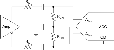 Figure 63. Biasing AC-Coupled ADC Inputs Using the ADC CM Output
The signal can be re-biased when ac coupling; thus, the output common-mode voltage of the amplifier is a don’t care for the ADC.
10.2.2.3.4 ADC Input Common-Mode Voltage Considerations—DC-Coupled Input
DC-coupled applications vary in complexity and requirements, depending on the ADC. One typical requirement is resolving the mismatch between the common-mode voltage of the driving amplifier and the ADC. Devices such as the ADS5424 require a nominal 2.4-V input common-mode, while other devices such as the ADS5485 require a nominal 3.1-V input common-mode; still others such as the ADS6149 and the ADS4149 require 1.5 V and
0.95 V, respectively. As shown in Figure 64, a resistor network can be used to perform a common-mode level shift. This resistor network consists of the amplifier series output resistors and pull-up or pull-down resistors to a reference voltage. This resistor network introduces signal attenuation that may prevent the use of the full-scale input range of the ADC. ADCs with an input common-mode closer to the typical 2.5-V LMH3401 output common-mode are easier to dc-couple, and require little or no level shifting.
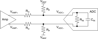 Figure 64. Resistor Network To DC Level-Shift Common-Mode Voltage
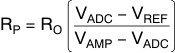
For common-mode analysis of the circuit in Figure 64, assume that VAMP± = VCM and VADC± = VCM (the specification for the ADC input common-mode voltage). VREF is chosen to be a voltage within the system higher than VCM (such as the ADC or amplifier analog supply) or ground, depending on whether the voltage must be pulled up or down, respectively; RO is chosen to be a reasonable value, such as 24.9 Ω. With these known values, RP can be found by using Equation 11:
Shifting the common-mode voltage with the resistor network comes at the expense of signal attenuation. Modeling the ADC input as the parallel combination of a resistance (RIN) and capacitance (CIN) using values taken from the ADC data sheet, the approximate differential input impedance (ZIN) for the ADC can be calculated at the signal frequency. The effect of CIN on the overall calculation of gain is typically minimal and can be ignored for simplicity (that is, ZIN = RIN). The ADC input impedance creates a divider with the resistor network; the gain (attenuation) for this divider can be calculated by Equation 12:
With ADCs that have internal resistors that bias the ADC input to the ADC input common-mode voltage, the effective RIN is equal to twice the value of the bias resistor. For example, the ADS5485 has a 1-kΩ resistor tying each input to the ADC VCM; therefore, the effective differential RIN is 2 kΩ.
The introduction of the RP resistors also modifies the effective load that must be driven by the amplifier. Equation 13 shows the effective load created when using the RP resistors.
The RP resistors function in parallel to the ADC input such that the effective load (output current) at the amplifier output is increased. Higher current loads limit the LMH3401 differential output swing.
Using the gain and knowing the full-scale input of the ADC (VADC FS), the required amplitude to drive the ADC with the network can be calculated using Equation 14:
As with any design, testing is recommended to validate whether the specific design goals are met.
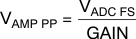
10.2.2.4 GSPS ADC Driver
The LMH3401 can drive the full Nyquist bandwidth of ADCs with sampling rates up to 4 GSPS, as shown in Figure 65. If the front-end bandwidth of the ADC is more than 2 GHz, use a simple noise filter to improve SNR. Otherwise, the ADC can be connected directly to the amplifier output pins. Matching resistors may not be required, however allow space for matching resistors on the preliminary design.
 Figure 65. GSPS ADC Driver
10.2.2.5 Common-Mode Voltage Correction
The LMH3401 can set the output common-mode voltage to within a typical value of ±30 mV. If greater accuracy is desired, a simple circuit can improve this accuracy by an order of magnitude. A precision, low-power operational amplifier is used to sense the error in the output common-mode of the LMH3401 and corrects the error by adjusting the voltage at the CM pin. In Figure 66, the precision of the op amp replaces the less accurate precision of the LMH3401 common-mode control circuit while still using the LMH3401 common-mode control circuit speed. The op amp in this circuit must have better than a 1-mV input-referred offset voltage and low noise. Otherwise the specifications are not very critical because the LMH3401 is responsible for the entire differential signal path.
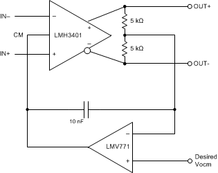 Figure 66. Common-Mode Correction Circuit
10.2.2.6 Active Balun
The LMH3401 is designed to convert single-ended, 50-Ω source impedance signals to a differential output with very high bandwidth and linearity, as shown in Figure 67. The LMH3401 can support dc coupling as well as ac coupling. The LMH3401 is smaller than any balun with low-frequency response and has balance errors that are excellent over a wide frequency range. As shown in Figure 68, the LMH3401 balance error is better than
–40 dBc up to 1 GHz when used with a 5-V supply.
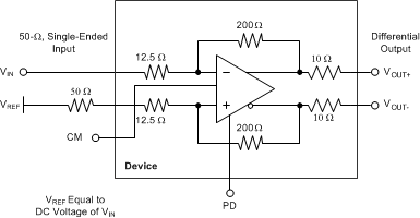 Figure 67. Active Balun
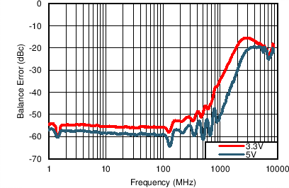 Figure 68. Balance Error
10.2.2.7 Application Curves
The LMH3401 has on-chip series output resistors to facilitate board layout. These resistors provide the LMH3401 extra phase margin in most applications. When the amplifier is used to drive a terminated transmission line or a controlled impedance filter, extra resistance is required to match the transmission line of the filter. In these applications, there is a 6 dB loss of gain. When the LMH3401 is used to drive loads that are not back-terminated there is a loss in gain resulting from the on-chip resistors. Figure 69 shows that loss for different load conditions. In most cases the loads are between 50 Ω and 200 Ω, where the on-chip resistor losses are 1.6 dB and 0.42 dB, respectively. Figure 70 shows the net gain realized by the amplifier for a large range of load resistances.
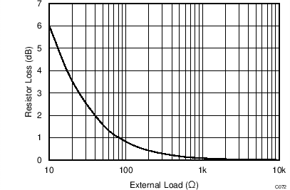 Figure 69. Gain Loss Due to On Chip Output Resistors
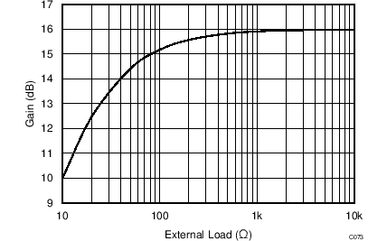 Figure 70. Net Gain versus Load Resistance
10.3 Do's and Don'ts
10.3.1 Do:
- Include a thermal design at the beginning of the project.
- Use well-terminated transmission lines for all signals.
- Use solid metal layers for the power supplies.
- Keep signal lines as straight as possible.
- Use split supplies where required.
10.3.2 Don't:
- Use a lower supply voltage than necessary.
- Use thin metal traces to supply power.
- Forget about the common-mode response of filters and transmission lines.