SBOS997 August 2020 – MONTH LMH9135
PRODUCTION DATA
- 1 Features
- 2 Applications
- 3 Description
- 4 Revision History
- 5 Pin Configuration and Functions
- 6 Specifications
- 7 Detailed Description
- 8 Application and Implementation
- 9 Power Supply Recommendations
- 10Layout
- 11Device and Documentation Support
- 12Mechanical, Packaging, and Orderable Information
Package Options
Mechanical Data (Package|Pins)
- RRL|12
Thermal pad, mechanical data (Package|Pins)
Orderable Information
8.2.1 Design Requirements
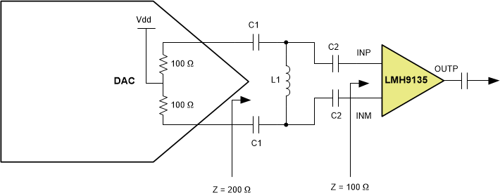
Input of LMH9135 is matched to 100 Ω and therefore can be directly driven by a DAC that has 100 Ω source impedance without any external matching network. If a DAC with different impedance is used, then it should be appropriately matched to get the best RF performance.
The example in Figure 8-2 shows how LMH9135 can be matched to a DAC that has 200-Ω differential termination.
 Figure 8-2 LMH9135 Driven by a DAC with 200-Ω Termination