SNAS577G February 2012 – August 2018 LMK00304
PRODUCTION DATA.
- 1 Features
- 2 Applications
- 3 Description
- 4 Revision History
- 5 Pin Configuration and Functions
- 6 Specifications
- 7 Parameter Measurement Information
- 8 Detailed Description
- 9 Application and Implementation
- 10Power Supply Recommendations
- 11Device and Documentation Support
- 12Mechanical, Packaging, and Orderable Information
Package Options
Mechanical Data (Package|Pins)
- RTV|32
Thermal pad, mechanical data (Package|Pins)
- RTV|32
Orderable Information
9.3.1 Termination for DC-Coupled Differential Operation
For DC-coupled operation of an LVDS driver, terminate with 100 Ω as close as possible to the LVDS receiver as shown in Figure 29.
 Figure 29. Differential LVDS Operation, DC Coupling,
No Biasing by the Receiver
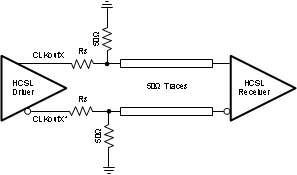
For DC-coupled operation of an HCSL driver, terminate with 50 Ω to ground near the driver output as shown in Figure 30. Series resistors, Rs, may be used to limit overshoot due to the fast transient current. Because HCSL drivers require a DC path to ground, AC coupling is not allowed between the output drivers and the 50-Ω termination resistors.
 Figure 30. HCSL Operation, DC Coupling
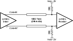
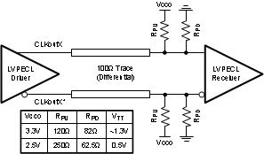
 For DC-coupled operation of an LVPECL driver, terminate with 50 Ω to Vcco - 2 V as shown in Figure 31. Alternatively terminate with a Thevenin equivalent circuit as shown in Figure 32 for Vcco (output driver supply voltage) = 3.3 V and 2.5 V. In the Thevenin equivalent circuit, the resistor dividers set the output termination voltage (VTT) to Vcco – 2 V.
 Figure 31. Differential LVPECL Operation, DC Coupling
  Figure 32. Differential LVPECL Operation, DC Coupling, Thevenin Equivalent