SNAS489K March 2011 – December 2014 LMK04803 , LMK04805 , LMK04806 , LMK04808
PRODUCTION DATA.
- 1 Features
- 2 Applications
- 3 Description
- 4 Revision History
- 5 Pin Configuration and Functions
- 6 Specifications
-
7 Parameter Measurement Information
- 7.1
Charge Pump Current Specification Definitions
- 7.1.1 Charge Pump Output Current Magnitude Variation Vs. Charge Pump Output Voltage
- 7.1.2 Charge Pump Sink Current Vs. Charge Pump Output Source Current Mismatch
- 7.1.3 Charge Pump Output Current Magnitude Variation vs. Ambient Temperature"Temperature" to "Ambient Temperature" in heading titled "Charge Pump Output Current Magnitude Variation vs. Ambient Temperature"
- 7.2 Differential Voltage Measurement Terminology
- 7.1
Charge Pump Current Specification Definitions
-
8 Detailed Description
- 8.1
Overview
- 8.1.1 System Architecture
- 8.1.2 PLL1 Redundant Reference Inputs (CLKin0/CLKin0* and CLKin1/CLKin1*)
- 8.1.3 PLL1 Tunable Crystal Support
- 8.1.4 VCXO/CRYSTAL Buffered Outputs
- 8.1.5 Frequency Holdover
- 8.1.6 Integrated Loop Filter Poles
- 8.1.7 Internal VCO
- 8.1.8 External VCO Mode
- 8.1.9 Clock Distribution
- 8.1.10 0-Delay
- 8.1.11 Default Startup Clocks
- 8.1.12 Status Pins
- 8.1.13 Register Readback
- 8.2 Functional Block Diagram
- 8.3
Feature Description
- 8.3.1 Serial MICROWIRE Timing Diagram
- 8.3.2 Advanced MICROWIRE Timing Diagrams
- 8.3.3 Inputs / Outputs
- 8.3.4 Input Clock Switching
- 8.3.5 Holdover Mode
- 8.3.6 PLLs
- 8.3.7 Status Pins
- 8.3.8 VCO
- 8.3.9
Clock Distribution
- 8.3.9.1 Fixed Digital Delay
- 8.3.9.2 Fixed Digital Delay - Example
- 8.3.9.3
Clock Output Synchronization (SYNC)
- 8.3.9.3.1 Effect of SYNC
- 8.3.9.3.2 Methods of Generating SYNC
- 8.3.9.3.3 Avoiding Clock Output Interruption Due to Sync
- 8.3.9.3.4 SYNC Timing
- 8.3.9.3.5
Dynamically Programming Digital Delay
- 8.3.9.3.5.1 Absolute vs. Relative Dynamic Digital Delay
- 8.3.9.3.5.2 Dynamic Digital Delay and 0-Delay Mode
- 8.3.9.3.5.3 SYNC and Minimum Step Size
- 8.3.9.3.5.4 Programming Overview
- 8.3.9.3.5.5 Internal Dynamic Digital Delay Timing
- 8.3.9.3.5.6 Other Timing Requirements
- 8.3.9.3.5.7 Absolute Dynamic Digital Delay
- 8.3.9.3.5.8 Relative Dynamic Digital Delay
- 8.3.10 0-Delay Mode
- 8.4 Device Functional Modes
- 8.5 Programming
- 8.6
Register Maps
- 8.6.1 Register Map and Readback Register Map
- 8.6.2 Default Device Register Settings After Power On Reset
- 8.6.3
Register Descriptions
- 8.6.3.1
Register R0 TO R5
- 8.6.3.1.1 CLKoutX_Y_PD, Powerdown CLKoutX_Y Output Path
- 8.6.3.1.2 CLKoutX_Y_OSCin_Sel, Clock Group Source
- 8.6.3.1.3 CLKoutY_ADLY_SEL[29], CLKoutX_ADLY_SEL[28], Select Analog Delay
- 8.6.3.1.4 CLKoutX_Y_DDLY, Clock Channel Digital Delay
- 8.6.3.1.5 Reset
- 8.6.3.1.6 POWERDOWN
- 8.6.3.1.7 CLKoutX_Y_HS, Digital Delay Half Shift
- 8.6.3.1.8 CLKoutX_Y_DIV, Clock Output Divide
- 8.6.3.2 Registers R6 TO R8
- 8.6.3.3
Register R10
- 8.6.3.3.1 OSCout1_LVPECL_AMP, LVPECL Output Amplitude Control
- 8.6.3.3.2 OSCout0_TYPE
- 8.6.3.3.3 EN_OSCoutX, OSCout Output Enable
- 8.6.3.3.4 OSCoutX_MUX, Clock Output Mux
- 8.6.3.3.5 PD_OSCin, OSCin Powerdown Control
- 8.6.3.3.6 OSCout_DIV, Oscillator Output Divide
- 8.6.3.3.7 VCO_MUX
- 8.6.3.3.8 EN_FEEDBACK_MUX
- 8.6.3.3.9 VCO_DIV, VCO Divider
- 8.6.3.3.10 FEEDBACK_MUX
- 8.6.3.4 Register R11
- 8.6.3.5 Register R12
- 8.6.3.6 Register R13
- 8.6.3.7 Register 14
- 8.6.3.8 REGISTER 15
- 8.6.3.9 Register 16
- 8.6.3.10 Register 23
- 8.6.3.11
Register 24
- 8.6.3.11.1 PLL2_C4_LF, PLL2 Integrated Loop Filter Component
- 8.6.3.11.2 PLL2_C3_LF, PLL2 Integrated Loop Filter Component
- 8.6.3.11.3 PLL2_R4_LF, PLL2 Integrated Loop Filter Component
- 8.6.3.11.4 PLL2_R3_LF, PLL2 Integrated Loop Filter Component
- 8.6.3.11.5 PLL1_N_DLY
- 8.6.3.11.6 PLL1_R_DLY
- 8.6.3.11.7 PLL1_WND_SIZE
- 8.6.3.12 Register 25
- 8.6.3.13 Register 26
- 8.6.3.14 REGISTER 27
- 8.6.3.15 Register 28
- 8.6.3.16 Register 29
- 8.6.3.17 Register 30
- 8.6.3.18 Register 31
- 8.6.3.1
Register R0 TO R5
- 8.1
Overview
-
9 Application and Implementation
- 9.1
Application Information
- 9.1.1 Loop Filter
- 9.1.2 Driving CLKin and OSCin Inputs
- 9.1.3 Termination and Use of Clock Output (Drivers)
- 9.1.4 Frequency Planning with the LMK0480x Family
- 9.1.5 PLL Programming
- 9.1.6 Digital Lock Detect Frequency Accuracy
- 9.1.7 Calculating Dynamic Digital Delay Values for any Divide
- 9.1.8 Optional Crystal Oscillator Implementation (OSCin/OSCin*)
- 9.1.9 Application Curves
- 9.2 Typical Applications
- 9.3 System Examples
- 9.4 Do's and Don'ts
- 9.1
Application Information
- 10Power Supply Recommendations
- 11Layout
- 12Device and Documentation Support
- 13Mechanical, Packaging, and Orderable Information
Package Options
Mechanical Data (Package|Pins)
- NKD|64
Thermal pad, mechanical data (Package|Pins)
- NKD|64
Orderable Information
9 Application and Implementation
NOTE
Information in the following applications sections is not part of the TI component specification, and TI does not warrant its accuracy or completeness. TI’s customers are responsible for determining suitability of components for their purposes. Customers should validate and test their design implementation to confirm system functionality.
9.1 Application Information
To assist customers in frequency planning and design of loop filters, Texas Instruments provides the Clock Design Tool and Clock Architect.
9.1.1 Loop Filter
Each PLL of the LMK0480x family requires a dedicated loop filter.
9.1.1.1 PLL1
The loop filter for PLL1 must be connected to the CPout1 pin. Figure 20 shows a simple 2-pole loop filter. The output of the filter drives an external VCXO module or discrete implementation of a VCXO using a crystal resonator and external varactor diode. Higher order loop filters may be implemented using additional external R and C components. It is recommended the loop filter for PLL1 result in a total closed loop bandwidth in the range of 10 Hz to 200 Hz. The design of the loop filter is application specific and highly dependent on parameters such as the phase noise of the reference clock, VCXO phase noise, and phase detector frequency for PLL1. TI's Clock Conditioner Owner’s Manual covers this topic in detail and Texas Instruments Clock Design Tool can be used to simulate loop filter designs for both PLLs. These resources may be found at:
http://www.ti.com/lsds/ti/analog/clocksandtimers/clocks_and_timers.page
9.1.1.2 PLL2
As shown in Figure 20, the charge pump for PLL2 is directly connected to the optional internal loop filter components, which are normally used only if either a third or fourth pole is needed. The first and second poles are implemented with external components. The loop must be designed to be stable over the entire application-specific tuning range of the VCO. The designer should note the range of KVCO listed in the table of Electrical Characteristics and how this value can change over the expected range of VCO tuning frequencies. Because loop bandwidth is directly proportional to KVCO, the designer should model and simulate the loop at the expected extremes of the desired tuning range, using the appropriate values for KVCO.
When designing with the integrated loop filter of the LMK0480x family, considerations for minimum resistor thermal noise often lead one to the decision to design for the minimum value for integrated resistors, R3 and R4.
Both the integrated loop filter resistors (R3 and R4) and capacitors (C3 and C4) also restrict the maximum loop bandwidth. However, these integrated components do have the advantage that they are closer to the VCO and can therefore filter out some noise and spurs better than external components. For this reason, a common strategy is to minimize the internal loop filter resistors and then design for the largest internal capacitor values that permit a wide enough loop bandwidth. In situations where spur requirements are very stringent and there is margin on phase noise, a feasible strategy would be to design a loop filter with integrated resistor values larger than their minimum value.
 Figure 20. PLL1 and PLL2 Loop Filters
9.1.2 Driving CLKin and OSCin Inputs
9.1.2.1 Driving CLKin Pins with a Differential Source
Both CLKin ports can be driven by differential signals. It is recommended that the input mode be set to bipolar (CLKinX_BUF_TYPE = 0) when using differential reference clocks. The LMK0480x family internally biases the input pins so the differential interface should be AC coupled. The recommended circuits for driving the CLKin pins with either LVDS or LVPECL are shown in Figure 21 and Figure 22.
 Figure 21. CLKinX/X* Termination for an LVDS Reference Clock Source
 Figure 22. CLKinX/X* Termination for an LVPECL Reference Clock Source
Finally, a reference clock source that produces a differential sine wave output can drive the CLKin pins using the following circuit. Note: the signal level must conform to the requirements for the CLKin pins listed in Electrical Characteristics.
 Figure 23. CLKinX/X* Termination for a Differential Sinewave Reference Clock Source
9.1.2.2 Driving CLKin Pins with a Single-Ended Source
The CLKin pins of the LMK0480x family can be driven using a single-ended reference clock source, for example, either a sine wave source or an LVCMOS/LVTTL source. Either AC coupling or DC coupling may be used. In the case of the sine wave source that is expecting a 50-Ω load, it is recommended that AC coupling be used as shown in Figure 24 with a 50-Ω termination.
NOTE
The signal level must conform to the requirements for the CLKin pins listed in Electrical Characteristics. CLKinX_BUF_TYPE in Register 11 is recommended to be set to bipolar mode (CLKinX_BUF_TYPE = 0).
 Figure 24. CLKinX/X* Single-Ended Termination
If the CLKin pins are being driven with a single-ended LVCMOS/LVTTL source, either DC coupling or AC coupling may be used. If DC coupling is used, the CLKinX_BUF_TYPE should be set to MOS buffer mode (CLKinX_BUF_TYPE = 1) and the voltage swing of the source must meet the specifications for DC coupled, MOS-mode clock inputs given in the table of Electrical Characteristics. If AC coupling is used, the CLKinX_BUF_TYPE should be set to the bipolar buffer mode (CLKinX_BUF_TYPE = 0). The voltage swing at the input pins must meet the specifications for AC coupled, bipolar mode clock inputs given in the table of Electrical Characteristics. In this case, some attenuation of the clock input level may be required. A simple resistive divider circuit before the AC coupling capacitor is sufficient.
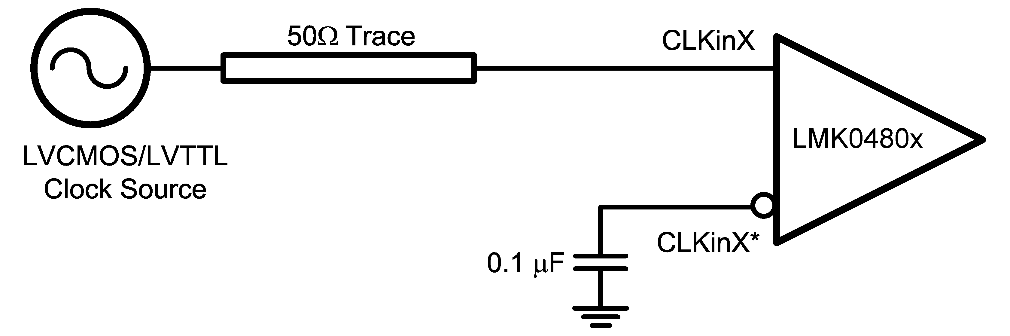 Figure 25. DC Coupled LVCMOS/LVTTL Reference Clock
9.1.3 Termination and Use of Clock Output (Drivers)
When terminating clock drivers keep in mind these guidelines for optimum phase noise and jitter performance:
- Transmission line theory should be followed for good impedance matching to prevent reflections.
- Clock drivers should be presented with the proper loads. For example:
- LVDS drivers are current drivers and require a closed current loop.
- LVPECL drivers are open emitters and require a DC path to ground.
- Receivers should be presented with a signal biased to their specified DC bias level (common mode voltage) for proper operation. Some receivers have self-biasing inputs that automatically bias to the proper voltage level. In this case, the signal should normally be AC coupled.
It is possible to drive a non-LVPECL or non-LVDS receiver with an LVDS or LVPECL driver as long as the above guidelines are followed. Check the datasheet of the receiver or input being driven to determine the best termination and coupling method to be sure that the receiver is biased at its optimum DC voltage (common mode voltage). For example, when driving the OSCin/OSCin* input of the LMK0480x family, OSCin/OSCin* should be AC coupled because OSCin/OSCin* biases the signal to the proper DC level (See Figure 39) This is only slightly different from the AC coupled cases described in Driving CLKin Pins with a Single-Ended Source because the DC blocking capacitors are placed between the termination and the OSCin/OSCin* pins, but the concept remains the same. The receiver (OSCin/OSCin*) sets the input to the optimum DC bias voltage (common mode voltage), not the driver.
9.1.3.1 Termination for DC Coupled Differential Operation
For DC coupled operation of an LVDS driver, terminate with 100 Ω as close as possible to the LVDS receiver as shown in Figure 26.
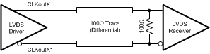 Figure 26. Differential LVDS Operation, DC Coupling, No Biasing of the Receiver
For DC coupled operation of an LVPECL driver, terminate with 50 Ω to VCC - 2 V as shown in Figure 27. Alternatively, terminate with a Thevenin equivalent circuit (120-Ω resistor connected to VCC and an 82-Ω resistor connected to ground with the driver connected to the junction of the 120-Ω and 82-Ω resistors) as shown in Figure 28 for VCC = 3.3 V.
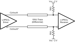 Figure 27. Differential LVPECL Operation, DC Coupling
 Figure 28. Differential LVPECL Operation, DC Coupling, Thevenin Equivalent
9.1.3.2 Termination for AC Coupled Differential Operation
AC coupling allows for shifting the DC bias level (common mode voltage) when driving different receiver standards. Since AC coupling prevents the driver from providing a DC bias voltage at the receiver it is important to ensure the receiver is biased to its ideal DC level.
When driving non-biased LVDS receivers with an LVDS driver, the signal may be AC coupled by adding DC blocking capacitors, however the proper DC bias point needs to be established at the receiver. One way to do this is with the termination circuitry in Figure 29.
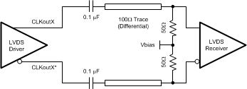 Figure 29. Differential LVDS Operation, AC Coupling,
 External Biasing at the Receiver
Some LVDS receivers may have internal biasing on the inputs. In this case, the circuit shown in Figure 29 is modified by replacing the 50-Ω terminations to Vbias with a single 100-Ω resistor across the input pins of the receiver, as shown in Figure 30. When using AC coupling with LVDS outputs, there may be a startup delay observed in the clock output due to capacitor charging. The previous figures employ a 0.1 µF capacitor. This value may need to be adjusted to meet the startup requirements for a particular application.
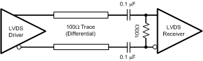 Figure 30. LVDS Termination for a Self-Biased Receiver
LVPECL drivers require a DC path to ground. When AC coupling an LVPECL signal use 120-Ω emitter resistors close to the LVPECL driver to provide a DC path to ground as shown in Figure 31. For proper receiver operation, the signal should be biased to the DC bias level (common mode voltage) specified by the receiver. The typical DC bias voltage for LVPECL receivers is 2 V. A Thevenin equivalent circuit (82-Ω resistor connected to VCC and a 120-Ω resistor connected to ground with the driver connected to the junction of the 82-Ω and 120-Ω resistors) is a valid termination as shown in Figure 31 for VCC = 3.3 V. Note this Thevenin circuit is different from the DC coupled example in Figure 28.
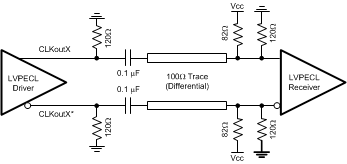 Figure 31. Differential LVPECL Operation, AC Coupling, Thevenin Equivalent,
 External Biasing at the Receiver
9.1.3.3 Termination for Single-Ended Operation
A balun can be used with either LVDS or LVPECL drivers to convert the balanced, differential signal into an unbalanced, single-ended signal.
It is possible to use an LVPECL driver as one or two separate 800 mVpp signals. When using only one LVPECL driver of a CLKoutX/CLKoutX* pair, be sure to properly terminate the unused driver. When DC coupling one of the LMK0480x family clock LVPECL drivers, the termination should be 50 Ω to VCC - 2 V as shown in Figure 32. The Thevenin equivalent circuit is also a valid termination as shown in Figure 33 for Vcc = 3.3 V.
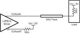 Figure 32. Single-Ended LVPECL Operation, DC Coupling
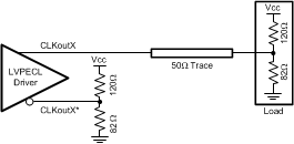 Figure 33. Single-Ended LVPECL Operation, DC Coupling,
 Thevenin Equivalent
When AC coupling an LVPECL driver use a 120-Ω emitter resistor to provide a DC path to ground and ensure a 50-Ω termination with the proper DC bias level for the receiver. The typical DC bias voltage for LVPECL receivers is 2 V (See Driving CLKin Pins with a Single-Ended Source). If the companion driver is not used it should be terminated with either a proper AC or DC termination. This latter example of AC coupling a single-ended LVPECL signal can be used to measure single-ended LVPECL performance using a spectrum analyzer or phase noise analyzer. When using most RF test equipment no DC bias point (0 VDC) is required for safe and proper operation. The internal 50-Ω termination of the test equipment correctly terminates the LVPECL driver being measured as shown in Figure 34.
 Figure 34. Single-Ended LVPECL Operation, AC Coupling
9.1.4 Frequency Planning with the LMK0480x Family
Calculating the value of the output dividers for use with the LMK0480x family is simple due to the architecture of the LMK0480x. That is, the VCO divider may be bypassed and the clock output dividers allow for even and odd output divide values from 2 to 1045. For most applications it is recommended to bypass the VCO divider.
The procedure for determining the needed LMK0480x device and clock output divider values for a set of clock output frequencies is straightforward.
- Calculate the least common multiple (LCM) of the clock output frequencies.
- Determine which VCO ranges will support the target clock output frequencies given the LCM.
- Determine the clock output divide values based on VCO frequency.
- Determine the PLL2_P, PLL2_N, and PLL2_R divider values given the OSCin VCXO or crystal frequency and VCO frequency.
For example, given the following target output frequencies: 200 MHz, 120 MHz, and 25 MHz with a VCXO frequency of 40 MHz:
- First determine the LCM of the three frequencies. LCM(200 MHz, 120 MHz, 25 MHz) = 600 MHz. The LCM frequency is the lowest frequency for which all of the target output frequencies are integer divisors of the LCM. Note: if there is one frequency which causes the LCM to be very large, greater than 3 GHz for example, determine if there is a single frequency requirement which causes this. It may be possible to select the VCXO/crystal frequency to satisfy this frequency requirement through OSCout or CLKout6/7/8/9 driven by OSCin. In this way it is possible to get non-integer related frequencies at the outputs.
- Second, since the LCM is not in a VCO frequency range supported by the LMK0480x family, multiply the LCM frequency by an integer which causes it to fall into a valid VCO frequency range of an LMK0480x device. In this case 600 MHz * 5 = 3000 MHz which is valid for the LMK04808.
-
Third, continuing the example by using a VCO frequency of 3000 MHz and the LMK04808, the CLKout dividers can be calculated by simply dividing the VCO frequency by the output frequency. To output 200 MHz, 120 MHz, and 25 MHz the output dividers will be 12, 20, and 96 respectively.
- 3000 MHz / 200 MHz = 15
- 3000 MHz / 120 MHz = 25
- 3000 MHz / 25 MHz = 120
- Fourth, PLL2 must be locked to its input reference. Refer to PLL Programming for more information on this topic. By programming the clock output dividers and the PLL2 dividers the VCO can lock to the frequency of 3000 MHz and the clock outputs dividers will each divide the VCO frequency down to the target output frequencies of 200 MHz, 120 MHz, and 25 MHz.
Refer to Application Note AN-1865, Frequency Synthesis and Planning for PLL Architectures (SNAA061) for more information on this topic and LCM calculations.
9.1.5 PLL Programming
To lock a PLL the divided reference and divided feedback from VCO or VCXO must result in the same phase detector frequency. The tables below illustrate how the divides are structured for the reference path (R) and feedback path (N) depending on the MODE of the device.
Table 113. PLL1 Phase Detector Frequency — Reference Path (R)
| MODE | PLL1 PDF (R) = |
|---|---|
| All | CLKinX Frequency / (CLKinX_PreR_DIV * PLL1_R) |
Table 114. PLL1 Phase Detector Frequency — Feedback Path (N)
| MODE | VCO_MUX | OSCout0 | PLL1 PDF (N) = |
|---|---|---|---|
| Dual PLL, Internal VCO | — | Bypass | VCXO Frequency / PLL1_N |
| — | Divided | VCXO Frequency / (OSCin_DIV * PLL1_N) | |
| Dual PLL, Internal VCO, 0-Delay | Bypass | — | VCO Frequency / (CLKoutX_Y_DIV * PLL1_N) (1) |
| Divided | — | VCO Frequency / (VCO_DIV * CLKoutX_Y_DIV * PLL1_N) (1) | |
| Dual PLL, External VCO, 0-Delay | — | — | VCO Frequency / (CLKoutX_Y_DIV * PLL1_N) (1) |
Table 115. PLL2 Phase Detector Frequency — Reference Path (R)
| EN_PLL2_REF_2X | PLL2 PDF (R) = |
|---|---|
| Disabled | OSCin Frequency / PLL2_R(1)(2) |
| Enabled | OSCin Frequency * 2 / PLL2_R(1)(2) |
Table 116. PLL2 Phase Detector Frequency — Feedback Path (N)
| MODE | VCO_MUX | PLL2 PDF (N) = |
|---|---|---|
| Dual PLL, Internal VCO | VCO | VCO Frequency / (PLL2_P * PLL2_N) |
| Dual PLL, Internal VCO, 0-Delay | ||
| Single PLL, Internal VCO | ||
| Dual PLL, Internal VCO | VCO Divider | VCO Frequency / (VCO_DIV * PLL2_P * PLL2_N) |
| Dual PLL, Internal VCO, 0-Delay | ||
| Single PLL, Internal VCO | ||
| Dual PLL, External VCO | — | VCO Frequency / (PLL2_P * PLL2_N) |
| Dual PLL External VCO, 0-Delay | ||
| Single PLL, External VCO | ||
| Single PLL, Internal VCO, 0-Delay | VCO | VCO Frequency / (CLKoutX_Y_DIV * PLL2_N) |
| VCO Divider | VCO Frequency / (VCO_DIV * CLKoutX_Y_DIV * PLL2_N) |
Table 117. PLL2 Phase Detector Frequency — Feedback Path (N) during VCO Frequency Calibration
| MODE | VCO_MUX | PLL2 PDF (N_CAL) = |
|---|---|---|
| All Internal VCO Modes | VCO | VCO Frequency / (PLL2_P * PLL2_N_CAL) |
| VCO Divider | VCO Frequency / (VCO_DIV * PLL2_P * PLL2_N_CAL) |
9.1.5.1 Example PLL2 N Divider Programming
To program PLL2 to lock an LMK04808 using Dual PLL mode to a VCO frequency of 3000 MHz using a 40 MHz VCXO reference, first determine the total PLL2 N divide value. This is VCO Frequency / PLL2 phase detector frequency. This example assumes the PLL2 reference frequency doubler is enabled and a PLL2 R divide value of 2 (see Note 1 in Table 115) which results in PLL2 phase detector frequency the same as PLL2 reference frequency (40 MHz). 3000 MHz / 40 MHz = 75, so the total PLL2 N divide value is 75.
The dividers in the PLL2 N feedback path for Dual PLL mode include PLL2_P and PLL2_N. PLL2_P can be programmed from 2 to 8 including both even and odd values. PLL2_N can be programmed from 1 to 263,143 including both even and odd values. Since the total PLL2 N divide value of 75 contains the factors 3, 5, and 5, it would be allowable to program PLL2_P to 3 or 5. It is simplest to use the smallest divide, so PLL2_P = 3, and PLL2_N = 25 which results in a Total PLL2 N = 75.
For this example and in most cases, PLL2_N_CAL will have the same value as PLL2_N. However when using Single PLL mode with 0-delay, the values will differ. When using an external VCO, PLL2_N_CAL value is unused.
To lock a PLL the divided reference and divided feedback from VCO or VCXO must result in the same phase detector frequency. The following tables illustrate how the divides are structured for the reference path (R) and feedback path (N) depending on the MODE of the device.
Table 118. PLL1 Phase Detector Frequency — Reference Path (R)
| MODE | (R) PLL1 PDF = |
|---|---|
| All | CLKinX Frequency / CLKinX_PreR_DIV / PLL1_R |
Table 119. PLL1 Phase Detector Frequency — Feedback Path (N)
| MODE | VCO_MUX | OSCout0 | PLL1 PDF (N) = |
|---|---|---|---|
| Internal VCO Dual PLL | — | Bypass | VCXO Frequency / PLL1_N |
| — | Divided | VCXO Frequency / OSCin_DIV / PLL1_N | |
| Internal VCO /w 0-delay | Bypass | — | VCO Frequency / CLKoutX_Y_DIV / PLL1_N (1) |
| Divided | — | VCO Frequency / VCO_DIV / CLKoutX_Y_DIV / PLL1_N (1) |
Table 120. PLL2 Phase Detector Frequency — Reference Path (R)
| EN_PLL2_REF_2X | PLL2 PDF (R) = |
|---|---|
| Disabled | OSCin Frequency / PLL2_R(1) |
| Enabled | OSCin Frequency * 2 / PLL2_R(1) |
Table 121. PLL2 Phase Detector Frequency — Feedback Path (N)
| MODE | VCO_MUX | PLL2 PDF (N) = |
|---|---|---|
| Dual PLL | VCO | VCO Frequency / PLL2_P / PLL2_N |
| Dual PLL /w 0-delay | ||
| Single PLL | ||
| Dual PLL | VCO Divider | VCO Frequency / VCO_DIV / PLL2_P / PLL2_N |
| Dual PLL /w 0-delay | ||
| Single PLL | ||
| Dual PLL External VCO | — | VCO Frequency / VCO_DIV / PLL2_P / PLL2_N |
| Dual PLL External VCO /w 0-delay | ||
| Single PLL /w 0-delay | VCO | VCO Frequency / CLKoutX_Y_DIV / PLL2_N |
| VCO Divider | VCO Frequency / VCO_DIV / CLKoutX_Y_DIV / PLL2_N |
Table 122. PLL2 Phase Detector Frequency — Feedback Path (N) during VCO Frequency Calibration
| MODE | VCO_MUX | PLL2 PDF (N_CAL) = |
|---|---|---|
| All Internal VCO Modes | VCO | VCO Frequency / PLL2_P / PLL2_N_CAL |
| VCO Divider | VCO Frequency / VCO_DIV / PLL2_P / PLL2_N_CAL | |
9.1.5.1.1 Example PLL2 N Divider Programming
To program PLL2 to lock an LMK04808 using Dual PLL mode to a VCO frequency of 3000 MHz using a 40-MHz VCXO reference, first determine the total PLL2 N divide value. This is VCO Frequency / PLL2 phase detector frequency. This example assumes a PLL2 R divide value of 1 which results in PLL2 phase detector frequency the same as PLL2 reference frequency (40 MHz). 3000 MHz / 40 MHz = 75, so the total PLL2 N divide value is 75.
The dividers in the PLL2 N feedback path for Dual PLL mode include PLL2_P and PLL2_N. PLL2_P can be programmed from 2 to 8, including both even and odd values. PLL2_N can be programmed from 1 to 263,143, including both even and odd values. Since the total PLL2 N divide value of 75 contains the factors 3, 5, and 5, it would be allowable to program PLL2_P to 3 or 5. It is simplest to use the smallest divide, so PLL2_P = 3, and PLL2_N = 25 which results in a Total PLL2 N = 75.
For this example and in most cases, PLL2_N_CAL will have the same value as PLL2_N. However when using Single PLL mode with 0-delay, the values will differ. When using an external VCO, PLL2_N_CAL value is unused.
9.1.6 Digital Lock Detect Frequency Accuracy
The digital lock detect circuit is used to determine PLL1 locked, PLL2 locked, and holdover exit events. A window size and lock count register are programmed to set a ppm frequency accuracy of reference to feedback signals of the PLL for each event to occur. When a PLL digital lock event occurs the PLL's digital lock detect is asserted true. When the holdover exit event occurs, the device will exit holdover mode.
Table 123. Digital Lock Detect Frequency Accuracy Table
| EVENT | PLL | WINDOW SIZE | LOCK COUNT |
|---|---|---|---|
| PLL1 Locked | PLL1 | PLL1_WND_SIZE | PLL1_DLD_CNT |
| PLL2 Locked | PLL2 | PLL2_WND_SIZE | PLL2_DLD_CNT |
| Holdover exit | PLL1 | PLL1_WND_SIZE | HOLDOVER_DLD_CNT |
For a digital lock detect event to occur there must be a “lock count” number of phase detector cycles of PLLX during which the time/phase error of the PLLX_R reference and PLLX_N feedback signal edges are within the user programmable "window size." Since there must be at least "lock count" phase detector events before a lock event occurs, a minimum digital lock event time can be calculated as "lock count" / fPDX where X = 1 for PLL1 or 2 for PLL2.
By using Equation 5, values for a "lock count" and "window size" can be chosen to set the frequency accuracy required by the system in ppm before the digital lock detect event occurs:
The effect of the "lock count" value is that it shortens the effective lock window size by dividing the "window size" by "lock count".
If at any time the PLLX_R reference and PLLX_N feedback signals are outside the time window set by "window size", then the “lock count” value is reset to 0.
9.1.7 Calculating Dynamic Digital Delay Values for any Divide
This section explains how to calculate the dynamic digital delay for any divide value.
Dynamic digital delay allows the time offset between two or more clock outputs to be adjusted with no or minimal interruption of clock outputs. Since the clock outputs are operating at a known frequency, the time offset can also be expressed as a phase shift. When dynamically adjusting the digital delay of clock outputs with different frequencies the phase shift should be expressed in terms of the higher frequency clock. The step size of the smallest time adjustment possible is equal to half the period of the Clock Distribution Path, which is the VCO frequency (Equation 3) or the VCO frequency divided by the VCO divider (Equation 4) if not bypassed. The smallest degree phase adjustment with respect to a clock frequency will be 360 * the smallest time adjustment * the clock frequency. The total number of phase offsets that the LMK0480x family is able to achieve using dynamic digital delay is equal 1 / (higher clock frequency * the smallest phase adjustment).
Equation 6 calculates the digital delay value that must be programmed for a synchronizing clock to achieve a 0 time/phase offset from the qualifying clock. Once this digital delay value is known, it is possible to calculate the digital delay value for any phase offset. The qualifying clock for dynamic digital delay is selected by the FEEDBACK_MUX. When dynamic digital delay is engaged with same clock output used for the qualifying clock and the new synchronized clock, it is termed relative dynamic digital delay since causing another SYNC event with the same digital delay value will offset the clock by the same phase once again. The important part of relative dynamic digital delay is that the CLKoutX_Y_HS must be programmed correctly when the SYNC event occurs (Table 6). This can result in needing to program the device twice. Once to set the new CLKoutX_Y_DDLY with CLKoutX_Y_HS as required for the SYNC event, and again to set the CLKoutX_Y_HS to its desired value.
Digital delay values are programmed using the CLKoutX_Y_DDLY and CLKoutX_Y_HS registers as shown in Equation 7. For example, to achieve a digital delay of 13.5, program CLKoutX_Y_DDLY = 14 and CLKoutX_Y_HS = 1.
Equation 6 uses the ceiling operator. To find the ceiling of a fractional number round up. An integer remains the same value.
Note: since the digital delay value for 0 time/phase offset is a function of the qualifying clock's divide value, the resulting digital delay value can be used for any clock output operating at any frequency to achieve a 0 time/phase offset from the qualifying clock. Therefore the calculated time shift table will also be the same as in Table 124.
9.1.7.1 Example
Consider a system with:
- A VCO frequency of 2000 MHz.
- The VCO divider is bypassed, therefore the clock distribution path frequency is 2000 MHz.
- CLKout0_1_DIV = 10 resulting in a 200 MHz frequency on CLKout0.
- CLKout2_3_DIV = 20 resulting in a 100 MHz frequency on CLKout2.
For this system the minimum time adjustment is 0.25 ns, which is 0.5 / (2000 MHz). Since the higher frequency is 200 MHz, phase adjustments will be calculated with respect to the 200 MHz frequency. The 0.25 ns minimum time adjustment results in a minimum phase adjustment of 18 degrees, which is 360 degrees / 200 MHz * 0.25 ns.
To calculate the digital delay value to achieve a 0 time/phase shift of CLKout2 when CLKout0 is the qualifying clock. Solve Equation 6 using the divide value of 10. To solve the equation 16/10 = 1.6, the ceiling of 1.6 is 2. Then to finish solving the equation solve (2 + 0.5) * 10 - 11.5 = 13.5. A digital delay value of 13.5 is programmed by setting CLKout2_3_DDLY = 14 and CLKout2_3_HS = 1.
To calculate the digital delay value to achieve a 0 time/phase shift of CLKout0 when CLKout2 is the qualifying clock, solve Equation 6 using the divide value of CLKout2, which is 20. This results in a digital delay of 18.5 which is programmed as CLKout0_1_DDLY = 19 and CLKout0_1_HS = 1.
Once the 0 time/phase shift digital delay programming value is known a table can be constructed with the digital delay value to be programmed for any time/phase offset by decrementing or incrementing the digital delay value by 0.5 for the minimum time/phase adjustment.
A complete filled out table for use of CLKout0 as the qualifying clock is shown in Table 124. It was created by entering a digital delay of 13.5 for 0 degree phase shift, then decrementing the digital delay down to the minimum value of 4.5. Since this did not result in all the possible phase shifts, the digital delay was then incremented from 13.5 to 14.0 to complete all possible phase shifts.
Table 124. Example Digital Delay Calculation
| DIGITAL DELAY |
CALCULATED TIME SHIFT (ns) |
RELATIVE TIME SHIFT to 200 MHz (ns) |
PHASE SHIFT of 200 MHz (Degrees) |
|---|---|---|---|
| 4.5 | -4.5 | 0.5 | 36 |
| 5 | -4.25 | 0.75 | 54 |
| 5.5 | -4.0 | 1.0 | 72 |
| 6 | -3.75 | 1.25 | 90 |
| 6.5 | -3.5 | 1.5 | 108 |
| 7 | -3.25 | 1.75 | 126 |
| 7.5 | -3.0 | 2.0 | 144 |
| 8 | -2.75 | 2.25 | 162 |
| 8.5 | -2.5 | 2.5 | 180 |
| 9 | -2.25 | 2.75 | 198 |
| 9.5 | -2.0 | 3.0 | 216 |
| 10 | -1.75 | 3.25 | 234 |
| 10.5 | -1.5 | 3.5 | 252 |
| 11 | -1.25 | 3.75 | 270 |
| 11.5 | -1.0 | 4.0 | 288 |
| 12 | -0.75 | 4.25 | 306 |
| 12.5 | -0.5 | 4.5 | 324 |
| 13 | -0.25 | 4.75 | 342 |
| 13.5 | 0 | 0 | 0 |
| 14 | 0.25 | 0.25 | 18 |
| 14.5 | 0.5 | 0.5 | 36 |
Observe that the digital delay value of 4.5 and 14.5 will achieve the same relative time shift/phase delay. However programming a digital delay of 14.5 will result in a clock off time for the synchronizing clock to achieve the same phase time shift/phase delay.
Digital delay value is programmed as CLKoutX_Y_DDLY - (0.5 * CLKoutX_Y_HS). So to achieve a digital delay of 13.5, program CLKoutX_Y_DDLY = 14 and CLKoutX_Y_HS = 1. To achieve a digital delay of 14, program CLKoutX_Y_DDLY = 14 and CLKoutX_Y_HS = 0.
9.1.8 Optional Crystal Oscillator Implementation (OSCin/OSCin*)
The LMK0480x family features supporting circuitry for a discretely implemented oscillator driving the OSCin port pins. Figure 35 illustrates a reference design circuit for a crystal oscillator:
 Figure 35. Reference Design Circuit for Crystal Oscillator Option
This circuit topology represents a parallel resonant mode oscillator design. When selecting a crystal for parallel resonance, the total load capacitance, CL, must be specified. The load capacitance is the sum of the tuning capacitance (CTUNE), the capacitance seen looking into the OSCin port (CIN), and stray capacitance due to PCB parasitics (CSTRAY), and is given by Equation 8.

CTUNE is provided by the varactor diode shown in Figure 35, Skyworks model SMV1249-074LF. A dual diode package with common cathode provides the variable capacitance for tuning. The single diode capacitance ranges from approximately 31 pF at 0.3 V to 3.4 pF at 3 V. The capacitance range of the dual package (anode to anode) is approximately 15.5 pF at 3 V to 1.7 pF at 0.3 V. The desired value of VTUNE applied to the diode should be VCC/2, or 1.65 V for VCC = 3.3 V. The typical performance curve from the data sheet for the SMV1249-074LF indicates that the capacitance at this voltage is approximately 6 pF (12 pF / 2).
The nominal input capacitance (CIN) of the LMK0480x family OSCin pins is 6 pF. The stray capacitance (CSTRAY) of the PCB should be minimized by arranging the oscillator circuit layout to achieve trace lengths as short as possible and as narrow as possible trace width (50 Ω characteristic impedance is not required).
As an example, assume that CSTRAY is 4 pF. The total load capacitance is nominally:
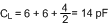
Consequently the load capacitance specification for the crystal in this case should be nominally 14 pF.
The 2.2-nF capacitors shown in the circuit are coupling capacitors that block the DC tuning voltage applied by the 4.7-kΩ and 10-kΩ resistors. The value of these coupling capacitors should be large, relative to the value of CTUNE (CC1 = CC2 >> CTUNE), so that CTUNE becomes the dominant capacitance.
For a specific value of CL, the corresponding resonant frequency (FL) of the parallel resonant mode circuit is:
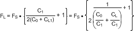
where
- FS = Series resonant frequency
- C1 = Motional capacitance of the crystal
- CL = Load capacitance
- C0 = Shunt capacitance of the crystal, specified on the crystal datasheet
The normalized tuning range of the circuit is closely approximated by:
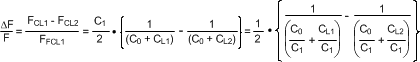
CL1, CL2 = The endpoints of the circuit’s load capacitance range, assuming a variable capacitance element is one component of the load. FCL1, FCL2 = parallel resonant frequencies at the extremes of the circuit’s load capacitance range.
A common range for the pullability ratio, C0/C1, is 250 to 280. The ratio of the load capacitance to the shunt capacitance is ~(n * 1000), n < 10. Hence, picking a crystal with a smaller pullability ratio supports a wider tuning range because this allows the scale factors related to the load capacitance to dominate.
Examples of the phase noise and jitter performance of the LMK04808 with a crystal oscillator are shown in Table 125. This table illustrates the clock output phase noise when a 20.48-MHz crystal is paired with PLL1. Performance of other LMK0480x devices will be similar.
Table 125. Example RMS Jitter and Clock Output Phase Noise for LMK04808
with a 20.48 MHz Crystal Driving OSCin (T = 25 °C, VCC = 3.3 V) (1)
Example crystal specifications are presented in Table 126.
Table 126. Example Crystal Specifications
| PARAMETER | VALUE |
|---|---|
| Nominal Frequency (MHz) | 20.48 |
| Frequency Stability, T = 25 °C | ± 10 ppm |
| Operating temperature range | -40 °C to +85 °C |
| Frequency Stability, -40 °C to +85 °C | ± 15 ppm |
| Load Capacitance | 14 pF |
| Shunt Capacitance (C0) | 5 pF Maximum |
| Motional Capacitance (C1) | 20 fF ± 30% |
| Equivalent Series Resistance | 25 Ω Maximum |
| Drive level | 2 mWatts Maximum |
| C0/C1 ratio | 225 typical, 250 Maximum |
See Figure 36 for a representative tuning curve.
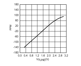 Figure 36. Example Tuning Curve, 20.48 MHz Crystal
The tuning curve achieved in the user's application may differ from the curve shown above due to differences in PCB layout and component selection.
This data is measured on the bench with the crystal integrated with the LMK0480x family. Using a voltmeter to monitor the VTUNE node for the crystal, the PLL1 reference clock input frequency is swept in frequency and the resulting tuning voltage generated by PLL1 is measured at each frequency. At each value of the reference clock frequency, the lock state of PLL1 should be monitored to ensure that the tuning voltage applied to the crystal is valid.
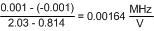
The curve shows over the tuning voltage range of 0.3 VDC to 3.0 VDC, the frequency range is -140 to +91 ppm; or equivalently, a tuning range of -2850 Hz to +1850 Hz. The measured tuning voltage at the nominal crystal frequency (20.48 MHz) is 1.7 V. Using the diode data sheet tuning characteristics, this voltage results in a tuning capacitance of approximately 6.5 pF.
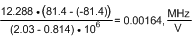
The tuning curve data can be used to calculate the gain of the oscillator (KVCO). The data used in the calculations is taken from the most linear portion of the curve, a region centered on the crossover point at the nominal frequency (20.48 MHz). For a well designed circuit, this is the most likely operating range. In this case, the tuning range used for the calculations is ± 1000 Hz (± 0.001 MHz), or ± 81.4 ppm. The simplest method is to calculate the ratio:
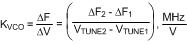
ΔF2 and ΔF1 are in units of MHz. Using data from the curve this becomes:
A second method uses the tuning data in units of ppm:
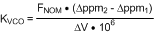
FNOM is the nominal frequency of the crystal and is in units of MHz. Using the data, this becomes:
In order to ensure startup of the oscillator circuit, the equivalent series resistance (ESR) of the selected crystal should conform to the specifications listed in the table of Electrical Characteristics.
It is also important to select a crystal with adequate power dissipation capability, or drive level. If the drive level supplied by the oscillator exceeds the maximum specified by the crystal manufacturer, the crystal will undergo excessive aging and possibly become damaged. Drive level is directly proportional to resonant frequency, capacitive load seen by the crystal, voltage and equivalent series resistance (ESR).
For more complete coverage of crystal oscillator design, see:
http://www.ti.com/lsds/ti/analog/clocksandtimers/tools.page or Application Note AN-1939, Crystal Based Oscillator Design with the LMK04000 Family (SNAA065).
9.1.9 Application Curves
See Figure 36 for a representative tuning curve.
9.2 Typical Applications
Normal use case of the LMK0480x device is as a dual loop jitter cleaner. This section will discuss a design example to illustrate the various functional aspects of the LMK0480x device.
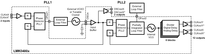 Figure 37. Simplified Functional Block Diagram for Dual Loop Mode
9.2.1 Design Requirements
Given a remote radio head (RRU) type application which needs to clock some ADCs, DACs, FPGA, SERDES, and an LO. The input clock will be a recovered clock which needs jitter cleaning. The FPGA clock should have a clock output on power up. A summary of clock input and output requirements are as follows:
Clock Input:
- 30.72 MHz recovered clock.
Clock Outputs:
- 2x 245.76 MHz clock for ADC, LVPECL
- 4x 983.04 MHz clock for DAC, LVPECL
- 1x 122.88 MHz clock for FPGA, LVPECL. POR clock
- 1x 122.88 MHz clock for SERDES, LVPECL
- 2x 122.88 MHz clock for LO, LVCMOS
It is also desirable to have the holdover feature engage if the recovered clock reference is ever lost. The following information reviews the steps to produce this design.
9.2.2 Detailed Design Procedure
Design of all aspects of the LMK0480x are quite involved and software has been written to assist in part selection, part programming, loop filter design, and simulation. This design procedure will give a quick outline of the process.
Note that this information is current as of the date of the release of this datasheet. Design tools receive continuous improvements to add features and improve model accuracy. Refer to software instructions or training for latest features.
- Device Selection
- the key to device selection is required VCO frequency given required output frequencies. The device must be able to produce the VCO frequency that can be divided down to required output frequencies.
- The software design tools will take inot account VCO frequency range for specific devices based on the application's required output frequencies. Using an external VCO provides increased flexibility regarding valid designs.
- To understand the process better, refer to Frequency Planning with the LMK0480x Family for more detail on calculating valid VCO frequency when using integer dividers using the least common multiple (LCM) of the output frequencies.
- Device Configuration
- There are many possible permutations of dividers and other registers to get same input and output frequencies from a device. However there are some optimizations and trade-offs to be considered.
- If more than one divider is in series, for instance VCO divider to CLKout divider, or VCO divider to PLL prescaler to PLL N. It is possible although not assured that some crosstalk/mixing could be created when using some divides.
- The design software normally attempts to maximize phase detector frequency, use smallest dividers, and maximizes PLL charge pump current.
- When an external VCXO or crystal is used for jitter cleaning, the design software will choose the maximum frequency value, depending on design software options, this max frequency may be limited to standard value VCXOs/Crystals. Note, depending on application, different frequency VCXOs may be chosen to generate some of the required output frequencies.
- Refer to PLL Programming for divider equations need to ensure PLL is locked. The design software is able to configure the device for most cases, but at this time for advanced features like 0-delay, the user must take care to ensure proper PLL programming.
- These guidelines may be followed when configuring PLL related dividers or other related registers:
- For lowest possible in-band PLL flat noise, maximize phase detector frequency to minimize N divide value.
- For lowest possible in-band PLL flat noise, maximize charge pump current. The highest value charge pump currents often have similar performance due to diminishing returns.
- To reduce loop filter component sizes, increase N value and/or reduce charge pump current.
- Large capacitors help reduce phase detector spurs at phase detector frequency caused by external VCOs/VCXOs with low input impedance.
- As rule of thumb, keeping the phase detector frequency approximately between 10 * PLL loop bandwidth and 100 * PLL loop bandwidth. A phase detector frequency less than 5 * PLL bandwidth may be unstable and a phase detector frequency > 100 * loop bandwidth may experience increased lock time due to cycle slipping.
- There are many possible permutations of dividers and other registers to get same input and output frequencies from a device. However there are some optimizations and trade-offs to be considered.
- PLL Loop Filter Design
- It is recommended to use Clock Design Tool or Clock Architect to design your loop filter.
- Best loop filter design and simulation can be achieved when:
- Custom reference and VCXO phase noise profiles are loaded into the software.
- VCO gain of the external VCXO or possible external VCO device are entered.
- The Clock Design Tool will return solutions with high reference/phase detector frequencies by default. In the Clock Design Tool the user may increase the reference divider to reduce the frequency if desired. Due to the narrow loop bandwidth used on PLL1, it is common to lower the phase detector frequency on PLL1 to reduce component size.
- While designing loop filter, adjusting the charge pump current or N value can help with loop filter component selection. Lower charge pump currents and larger N values result in smaller component values but may increase impacts of leakage and reduce PLL phase noise performance.
- More detailed understanding of loop filter design can found in Dean Banerjee's PLL Performance, Simulation, and Design (www.ti.com/tool/pll_book).
- Clock Output Assignment
- At this time the design software does not take into account frequency assignment to specific outputs except to ensure that the output frequencies can be achieved. It is best to consider proximity of each clock output to each other and other PLL circuitry when choosing final clock output locations. Here are some guidelines to help achieve best performance when assigning outputs to specific CLKout/OSCout pins.
- Group common frequencies together.
- PLL charge pump circuitry can cause crosstalk at charge pump frequency. Place outputs sharing charge pump frequency or lower priority outputs not sensitive to charge pump frequency spurs together.
- Muxes can create a path for noise coupling. Consider all frequencies which may have some bleed through from non-selected mux inputs.
- For example, LMK0480x CLKout6/7 and CLKout8/9 share a mux with OSCin.
- Some clock targets require low close-in phase noise. If possible, use a VCXO based PLL1 output for such a clock target. An example is a clock to a PLL reference.
- Some clock targets require excellent noise floor performance. Outputs driven by the internal VCO have the best noise floor performance. An example is an ADC or DAC.
- At this time the design software does not take into account frequency assignment to specific outputs except to ensure that the output frequencies can be achieved. It is best to consider proximity of each clock output to each other and other PLL circuitry when choosing final clock output locations. Here are some guidelines to help achieve best performance when assigning outputs to specific CLKout/OSCout pins.
- Other device specific configuration. For LMK0480x, consider the following:
- PLL lock time based on programming:
- In addition to the time it takes the device to lock to frequency, there is a digital filter to avoid false lock time detects which can also be used to ensure a specific PPM frequency accuracy. This also impacts the time it takes for the digital lock detect (DLD) pin to be asserted. Refer to Digital Lock Detect Frequency Accuracy for more information.
- Holdover configuration:
- Specific PPM frequency accuracy required to exit holdover can be programmed. Refer to Digital Lock Detect Frequency Accuracy for more information.
- Digital delay: phase alignment of the output clocks.
- Analog delay: another method to shift phases of clocks with finer resolution with the penalty of increase noise floor. Clock Design Tool can simulate analog delay impact on phase noise floor.
- Dynamic digital delay: ability to shift phase alignment of clocks with minimum disruption during operation.
- PLL lock time based on programming:
- Device Programming
- The software tool CodeLoader for EVM programming can be used to setup the device in the desired configuration, then export a hex register map suitable for use in application.
Some additional information on each part of the design procedure for the RRU example is below.
9.2.2.1 Device Selection
Use the WEBENCH Clock Architect Tool or Clock Design Tool. Enter the required frequencies and formats into the tool. To use this device, find a solution using the LMK04808B.
9.2.2.1.1 Clock Architect
When viewing resulting solutions, it is possible to narrow the parts used in the solution by setting a filter.
Under advanced tab, filtering of specific parts can be done using regular expressions in the Part Filter box. "LMK04808B" will filter for only the LMK04808B devices (without quotes).
9.2.2.1.2 Clock Design Tool
In wizard-mode, select Dual Loop PLL to find the LMK04808B device. If a high frequency and clean reference is available, Although dual loop mode is selected as a customer requirement, it is not required to use dual loop; PLL1 can be powered down and input is then provided via the OSCin port. When simulating single loop solutions, set PLL1 loop filter block to "0 Hz LBW" and use VCXO as the reference block.
9.2.2.1.3 Calculation Using LCM
In this example, the LCM(245.76 MHz, 983.04 MHz, 122.88 MHz) = 983.04 MHz. A valid VCO frequency for LMK0480x is 2949.12 MHz = 3 * 983.04 MHz. Therefore the LMK0480B may be used to produce these output frequencies.
9.2.2.2 Device Configuration
The tools automatically configure the simulation to meet the input and output frequency requirements given and make assumptions about other parameters to give some default simulations. The assumptions made are to maximize input frequencies, phase detector frequencies, and charge pump currents while minimizing VCO frequency and divider values.
For this example, when using the clock design tool, the reference would have been manually entered as 30.72 MHz according to input frequency requirements, but the tool allows VCXO1 frequency either to be set manually, auto-selected according to standard frequencies, or auto-selected for best frequency. With the best frequency option, the highest possible VCXO frequency which gives the highest possible PLL2 PDF frequency is recommended first. In this case: 421 + 53/175 MHz VCXO resulting in a 140 + 76/175 MHz phase detector frequency. This is a high phase detector frequency, but the VCXO is likely going to be a custom order. The select configuration page just before simulation shows before some different configurations possible with different VCO divider values. For example, a more common 491.52 MHz frequency provides a 122.88 MHz PDF. This is a more logical configuration.
From the simulation page of clock design tool, it can be seen that the VCXO frequency of 491.52 MHz is too high for feedback into the PLL1_N divider. Reducing the VCXO frequency to 245.76 MHz resolves the PLL1_N divider max input frequency problem. The PLL2 R divider must be updated to 2 so that the VCO of PLL2 is still at 2949.12 MHz.
At this point the design meets all input and output frequency requirements and it is possible to design a loop filter for system and simulate performance on CLKouts. However, consider also the following:
- At this time the clock design tool doesn't assign outputs strategically for jitter, such as PLL1 vs PLL2. If PLL1 output frequency is high enough, it may have improved jitter performance depending on the noise floor and application required integration range.
- The clock design tool does not consider power on reset clocks in the clock requirements or assignments.
- The clock design tool simplifies the LMK0480x architecture not showing the mux complexity around OSCout0/1 and not showing OSCout1. Simulation of OSCout0 is equivalent to OSCout1.
9.2.2.2.1 PLL LO Reference
PLL1 outputs have the best phase noise performance for LO references. As such OSCout0 can be used to provide the 122.88 MHz LO reference clock. To achieve this with the 245.76 MHz VCXO the OSCout_DIV can be set to 2 to provide 122.88 MHz at OSCout0. However in the next section it is determined that for the POR clock, a 122.88 MHz VCXO will be chosen which results not needing to change this parameter.
9.2.2.2.2 POR Clock
If OSCout1 is to be used for LVPECL POR 122.88 MHz clock, the POR value of the OSCout_DIV is 1, so a 122.88 MHz VCXO frequency must be chosen. This may be desired anyway since the phase detector frequency is limited to 122.88 MHz and lower frequency VCXOs tend to cost less. With this change the OSCin frequency and phase detector frequency are the same, so the doubler must be enabled and the PLL2 R divider programmed = 2 to follow the rule stated in PLL2 Frequency Doubler. Since the clock design tool does not show the doubler, PLL2_R will still reflect the value 1 one for the simulation purposes.
If LVDS was required for POR clock, a voltage divider could be used to convert from LVPECL to LVDS.
Note: it is possible to set the PLL2 R = 0.5 to simulate the doubler in-case lower frequency VCXOs would like to be simulated. For example a 61.44 MHz VCXO could be used while retaining a 122.88 MHz phase detector frequency. However, it would reduce the LO reference frequency and POR clock frequency to 61.44 MHz.
At this time the main design updates have been made to support the POR clock and loop filter design may begin.
9.2.2.3 PLL Loop Filter Design
The PLL structure for the LMK0480x is illustrated in Loop Filter.
At this time the user may choose to make adjustments to the simulation tools for more accurate simulations to their application. For example:
- Clock Design Tool allows loading a custom phase noise plot for any block. Typically, a custom phase noise plot is entered for CLKin to match the reference phase noise to the device; a phase noise plot for the VCXO can additionally be provided to match the performance of VCXO used. For improved accuracy in simulation and optimum loop filter design, be sure to load these custom noise profiles for use in application. After loading a phase noise plot, user should recalculate the recommended loop filter design.
- The Clock Design Tool will return solutions with high reference/phase detector frequencies by default. In the Clock Design Tool the user may increase the reference divider to reduce the frequency if desired. Due to the narrow loop bandwidth used on PLL1, it is common to reduce the phase detector frequency on PLL1 by increasing PLL1 R.
For this example, for PLL1 to perform jitter cleaning and to minimize jitter from PLL2 used for frequency multiplication:
- PLL1: A narrow loop bandwidth PLL1 filter was design by updating the loop bandwidth to 50 Hz and phase margin to 50 degrees.
- PLL2:
- VCXO noise profile is measured, then loaded into VCXO block in clock design tool.
- The recommended loop filter is redesigned. Updates to the PLL1 loop filter and VCXO phase noise may change the loop filter recommendation.
The next two sections will discuss PLL1 and PLL2 loop filter design specific to this example using default phase noise profiles.
NOTE
Clock Design Tool provides some recommend loop filters upon first load of the simulation. Anytime PLL related inputs change like an input phase noise, charge pump current, divider values, and so forth. it is best to re-design the PLL1 loop filter to the recommended design or your desired parameters. After PLL1, then update the PLL2 loop filter in the same way to keep the loop filters designed and optimized for the application. Since PLL1 loop filter design may impact PLL2 loop filter design, be sure to update the designs in order.
9.2.2.3.1 PLL1 Loop Filter Design
For this example, in the clock design tool simulator click on the PLL1 loop filter design button, then update the loop bandwidth for 0.05 kHz and the phase margin for 50 degrees and press calculate. With the 30.72 MHz phase detector frequency and 1.6 mA charge pump; the designed loop filter's largest capacitor, C2, is 27 µF. Supposing a goal of < 10 µF; setting PLL1 R = 4 and pressing the calculate again shows that C2 is 6.8 µF. Suppose that a reduction to < 1 µF is desired, continuing to increase the PLL1 R to 8 resulting in a phase detector frequency of 3.84 MHz and reducing the charge pump current from 1.6 mA to 0.4 mA and calculating again shows that C2 is 820 nF. As N was increased and charge pump decreased, this final design has R2 = 12 kΩ. The first design with low N value and high charge pump current result in R2 = 390 Ω. The impact of the thermal resistance is calculated in the tool. Viewing the simulation of the loop filter with the 12-kΩ resistor shows that the thermal noise in the loop is not impacting performance.
It may be desired to design a 3rd order loop filter for additional attenuation input noise and spurs
With the PLL1 loop filter design complete, PLL2's loop filter is ready to be designed.
9.2.2.3.2 PLL2 Loop Filter Design
In the clock design tool simulator, click on the PLL2 loop filter design button, then press recommend design. For PLL2's loop filter maximum phase detector frequency and maximum charge pump current are typically used. Typically the jitter integration bandwidth includes the loop filter bandwidth for PLL2. The recommended loop filter by the tools are designed to minimize jitter. The integrated loop filter components are minimized with this recommendation as to allow maximum flexibility in achieve wide loop bandwidths for low PLL noise. With the recommended loop filter calculated, this loop filter is ready to be simulated.
If using integrated components is desired, open the bode plot for the PLL2 Loop Filter, then make adjustments to the integrated components. The effective loop bandwidth and phase margin with these updates is calculated. The integrated loop filter components are good to use when attempting to eliminate some spurs since they provide filtering after the bond wires. The recommended procedure is to increase C3/C4 capacitance, then R3/R4 resistance. Large R3/R4 resistance can result in degraded VCO phase noise performance.
9.2.2.4 Clock Output Assignment
At this time the Clock Design Tool and Clock Architect only assign outputs to specific clock outputs numerically; not necessarily by optimum configuration. The user may wish to make some educated re-assignment of outputs.
During device configuration, some output assignment was discussed since it impacted the part's configuration relating to loop filter design, such as:
- In this example, OSCout1 can be used to provide the power on reset (POR) start-up clock to the FPGA at 122.88 MHz since the VCXO frequency is the required output frequency.
- Since PLL1 outputs have best in-band noise, OSCout0 is used to provide LVCMOS output to the PLL reference for the LO. LVCMOS (Norm/Inv) is used instead of LVCMOS (Norm/Norm) to reduce crosstalk. It is also possible to use CLKout6/7 or CLKout8/9 for a PLL reference being driven from the VCXO. The noise floor will be higher, but close-in noise is typically of more concern since noise above the loop bandwidth of the LO will be dominated by the VCO of the LO. See Figure 38.
Since CLKout6/7 and CLKout8/9 have a mux allowing them to be driven by the VCXO and due there is a chance for some 122.88 MHz crosstalk from the VCXO. The 122.88 MHz SERDES clock will be placed on CLKout6 since it will not be sensitive to crosstalk as it is operating at the same frequency.
The two 245.76 MHz clocks and four 983.04 MHz clocks for the converters need to be discussed. There is some flexibility in assignment. For example CLKout0/1 could operate at 245.76 MHz for the ADCs and then CLKout2/3 and CLKout4/5 could operate at 983.04 MHz for the DAC. It is also possible to consider CLKout2/3 for the ADC and position CLKout0/1 and CLKout10/11 for the DAC. The ADCs clock was placed as far as possible from other clock which could result in sub-harmonic spurs since the ADC clock is often the most sensitive.
9.2.2.5 Other Device Specific Configuration
9.2.2.5.1 Digital Lock Detect
Digital lock time for PLL1 will ultimately depend upon the programming of the PLL1_DLD_CNT register as discussed in Digital Lock Detect Frequency Accuracy. Since the PLL1 phase detector frequency in this example is 3.84 MHz, the lock time will = 1 / (PLL1_DLD_CNT * 3.84 MHz)
Digital lock time for PLL1 if PLL1_DLD_CNT = 10000 is just over 2.6 ms. When using holdover, it is very important to program the PLL1_DLD_CNT to a value large enough to prevent false digital lock detect signals.
If PLL1_DLD_CNT is too small, when the device exits holdover and is re-locking, the DLD will go high while the phase of the reference and feedback are within the specified window size because the programmed PLL1_DLD_CNT will be satisfied. However, if the loop has not yet settled to without the window size, when the phases of the reference and feedback once again exceed the window size, the DLD will return low. Provided that DISABLE_DLD1_DET = 0, the device once again enter holdover. Assuming that the reference clock is valid because holdover was just exited, the exit criteria will again be met, holdover will exit, and PLL1 will start locking. Unfortunately, the same sequence of events will repeat resulting in oscillation out-of and back-into holdover. Setting the PLL1_DLD_CNT to an appropriately large value prevents chattering of the PLL1 DLD signal and stable holdover operation can be achieved.
Refer to Digital Lock Detect Frequency Accuracy for more detail on calculating exit times and how the PLL1_DLD_CNT and PLL1_WND_SIZE work together.
9.2.2.5.2 Holdover
For this example, when the recovered clock is lost, the goal is to set the VCXO to Vcc/2 until the recovered clock returns. Holdover Mode contains detailed information on how to program holdover.
To achieve the above goal, fixed holdover will be used. Program:
- HOLDOVER_MODE = 2 (Holdover enabled)
- EN_TRACK = 0 (Tracking disabled)
- EN_MAN_DAC = 1 (Use manual DAC for holdover voltage value)
- MAN_DAC = 512 (Approximately Vcc/2)
- DISABLE_DLD1_DET = 0 (Use PLL1 DLD = Low to start holdover)
9.2.2.6 Device Programming
The CodeLoader software is used to program the LMK0480x evaluation board using the LMK04808B profile. It also allows the exporting of a register map which can be used to program the device to the user’s desired configuration.
Once a configuration of dividers has been achieved using the Clock Design Tool to meet the requested input/output frequencies with the desired performance, the CodeLoader software is manually updated with this information to meet the required application. At this time no automatic import exists.
9.2.3 Application Curve
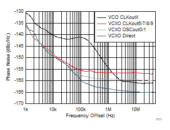
Illustration of Different Performance Depending on Signal Path.
9.3 System Examples
9.3.1 System Level Diagram
Figure 39 and Figure 40 show an LMK0480x family device with external circuitry for clocking and for power supply to serve as a guideline for good practices when designing with the LMK0480x family. Refer to Pin Connection Recommendations for more details on the pin connections and bypassing recommendations. Also refer to the evaluation board in LMK0480x Evaluation Board Instructions (SNAU076). PCB design will also play a role in device performance.
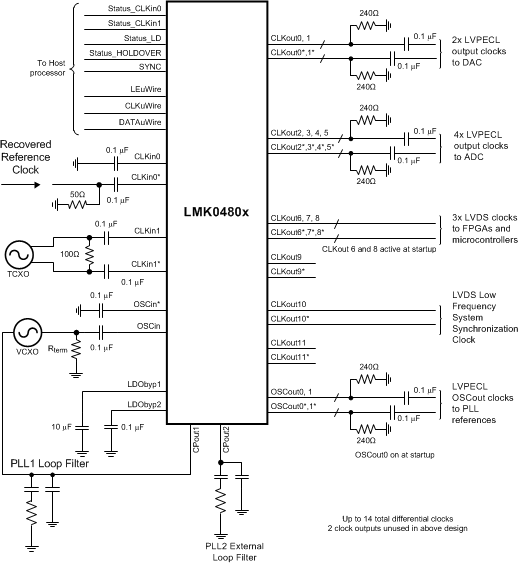 Figure 39. Example Application – System Schematic Except for Power
Figure 39 shows the primary reference clock input is at CLKin0/0*. A secondary reference clock is driving CLKin1/1*. Both clocks are depicted as AC coupled drivers. The VCXO attached to the OSCin/OSCin* port is configured as an AC coupled single-ended driver. Any of the input ports (CLKin0/0*, CLKin1/1*, or OSCin/OSCin*) may be configured as either differential or single-ended. These options are discussed later in the data sheet.
See Loop Filter for more information on PLL1 and PLL2 loop filters.
All the LVPECL clock outputs are AC coupled with 0.1 uF capacitors. The LVDS outputs are DC coupled.. Some clock outputs are depicted as LVPECL with 240-Ω emitter resistors and some clock outputs as LVDS. The appropriate output termination on each output should be implemented according to the output format to be programmed by the user. Later sections of this data sheet illustrate alternative methods for AC coupling, DC coupling and terminating the clock outputs.
PCB design will influence crosstalk performance. Tightly coupled clock traces will have less crosstalk than loosely coupled clock traces. Also proximity to other clocks traces will influence crosstalk.
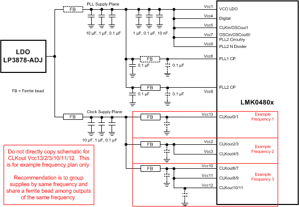
Figure 40 shows an example decoupling and bypassing scheme for the LMK0480x, which could apply to configurations shown in Figure 20 or Figure 39. Components drawn in dotted lines are optional (see Pin Connection Recommendations). Two power planes are used in these example designs, one for the clock outputs and one for PLL circuits. It is possible to reduce the number of decoupling components by tying together clock output Vcc pins for CLKouts that share the same frequency or otherwise can tolerate potential crosstalk between outputs with different frequencies. In the two examples, Vcc2 and Vcc3 can be tied together since CLKout2/3 and CLKout4/5 will operate at the same frequencies. Vcc10, Vcc11, and Vcc12 can be tied together since potential crosstalk between the FPGA/SerDes clocks and low-frequency synchronization clocks will not impact the performance of these digital interfaces, which typically have less stringent jitter requirements. PCB design will influence impedance to the supply. Vias and traces will increase the impedance to the power supply. Ensure good direct return current paths.
9.4 Do's and Don'ts
9.4.1 LVCMOS Complementary vs. Non-Complementary Operation
- It is recommended to use a complementary LVCMOS output format such as LVCMOS (Norm/Inv) to reduce switching noise and crosstalk when using LVCMOS.
- If only a single LVCMOS output is required, the complementary LVCMOS output format can still be used by leaving the unused LVCMOS output floating.
- A non-complimentary format such as LVCMOS (Norm/Norm) is not recommended as increased switching noise is present.
9.4.2 LVPECL Outputs
When using an LVPECL output it is not recommended to place a capacitor to ground on the output as might be done when using a capacitor input LC lowpass filter. The capacitor will appear as a short to the LVPECL output drivers which are able to supply large amounts of switching current. The effect of the LVPECL sourcing large switching currents can result in the following:
- Large switching currents through the Vcc pin of the LVPECL power supply resulting in more Vcc noise and possible Vcc spikes.
- Large switching currents injected into the ground plane through the capacitor which could couple onto other Vcc pins with bypass capacitors to ground resulting in more Vcc noise and possible Vcc spikes.