SNAS605AS March 2013 – May 2020 LMK04821 , LMK04826 , LMK04828
PRODUCTION DATA.
- 1 Features
- 2 Applications
- 3 Description
- 4 Revision History
- 5 Device Comparison Table
- 6 Pin Configuration and Functions
- 7 Specifications
- 8 Parameter Measurement Information
-
9 Detailed Description
- 9.1
Overview
- 9.1.1 Jitter Cleaning
- 9.1.2 JEDEC JESD204B Support
- 9.1.3 Three PLL1 Redundant Reference Inputs
- 9.1.4 VCXO/Crystal Buffered Output
- 9.1.5 Frequency Holdover
- 9.1.6 PLL2 Integrated Loop Filter Poles
- 9.1.7 Internal VCOs
- 9.1.8 External VCO Mode
- 9.1.9 Clock Distribution
- 9.1.10 Zero-Delay
- 9.1.11 Status Pins
- 9.2 Functional Block Diagram
- 9.3 Feature Description
- 9.4 Device Functional Modes
- 9.5 Programming
- 9.6 Register Maps
- 9.7
Device Register Descriptions
- 9.7.1 System Functions
- 9.7.2
(0x100 - 0x138) Device Clock and SYSREF Clock Output Controls
- 9.7.2.1 CLKoutX_Y_ODL, CLKoutX_Y_IDL, DCLKoutX_DIV
- 9.7.2.2 DCLKoutX_DDLY_CNTH, DCLKoutX_DDLY_CNTL
- 9.7.2.3 DCLKoutX_ADLY, DCLKoutX_ADLY_MUX, DCLKout_MUX
- 9.7.2.4 DCLKoutX_HS, SDCLKoutY_MUX, SDCLKoutY_DDLY, SDCLKoutY_HS
- 9.7.2.5 SDCLKoutY_ADLY_EN, SDCLKoutY_ADLY
- 9.7.2.6 DCLKoutX_DDLY_PD, DCLKoutX_HSg_PD, DCLKout_ADLYg_PD, DCLKout_ADLY_PD, DCLKoutX_Y_PD, SDCLKoutY_DIS_MODE, SDCLKoutY_PD
- 9.7.2.7 SDCLKoutY_POL, SDCLKoutY_FMT, DCLKoutX_POL, DCLKoutX_FMT
- 9.7.3
SYSREF, SYNC, and Device Config
- 9.7.3.1 VCO_MUX, OSCout_MUX, OSCout_FMT
- 9.7.3.2 SYSREF_CLKin0_MUX, SYSREF_MUX
- 9.7.3.3 SYSREF_DIV[12:8], SYSREF_DIV[7:0]
- 9.7.3.4 SYSREF_DDLY[12:8], SYSREF_DDLY[7:0]
- 9.7.3.5 SYSREF_PULSE_CNT
- 9.7.3.6 PLL2_NCLK_MUX, PLL1_NCLK_MUX, FB_MUX, FB_MUX_EN
- 9.7.3.7 PLL1_PD, VCO_LDO_PD, VCO_PD, OSCin_PD, SYSREF_GBL_PD, SYSREF_PD, SYSREF_DDLY_PD, SYSREF_PLSR_PD
- 9.7.3.8 DDLYdSYSREF_EN, DDLYdX_EN
- 9.7.3.9 DDLYd_STEP_CNT
- 9.7.3.10 SYSREF_CLR, SYNC_1SHOT_EN, SYNC_POL, SYNC_EN, SYNC_PLL2_DLD, SYNC_PLL1_DLD, SYNC_MODE
- 9.7.3.11 SYNC_DISSYSREF, SYNC_DISX
- 9.7.3.12 Fixed Registers (0x145, 0x171 - 0x172)
- 9.7.4 (0x146 - 0x149) CLKin Control
- 9.7.5 RESET_MUX, RESET_TYPE
- 9.7.6
(0x14B - 0x152) Holdover
- 9.7.6.1 LOS_TIMEOUT, LOS_EN, TRACK_EN, HOLDOVER_FORCE, MAN_DAC_EN, MAN_DAC[9:8]
- 9.7.6.2 MAN_DAC[9:8], MAN_DAC[7:0]
- 9.7.6.3 DAC_TRIP_LOW
- 9.7.6.4 DAC_CLK_MULT, DAC_TRIP_HIGH
- 9.7.6.5 DAC_CLK_CNTR
- 9.7.6.6 CLKin_OVERRIDE, HOLDOVER_PLL1_DET, HOLDOVER_LOS_DET, HOLDOVER_VTUNE_DET, HOLDOVER_HITLESS_SWITCH, HOLDOVER_EN
- 9.7.6.7 HOLDOVER_DLD_CNT[13:8], HOLDOVER_DLD_CNT[7:0]
- 9.7.7
(0x153 - 0x15F) PLL1 Configuration
- 9.7.7.1 CLKin0_R[13:8], CLKin0_R[7:0]
- 9.7.7.2 CLKin1_R[13:8], CLKin1_R[7:0]
- 9.7.7.3 CLKin2_R[13:8], CLKin2_R[7:0]
- 9.7.7.4 PLL1_N
- 9.7.7.5 PLL1_WND_SIZE, PLL1_CP_TRI, PLL1_CP_POL, PLL1_CP_GAIN
- 9.7.7.6 PLL1_DLD_CNT[13:8], PLL1_DLD_CNT[7:0]
- 9.7.7.7 PLL1_R_DLY, PLL1_N_DLY
- 9.7.7.8 PLL1_LD_MUX, PLL1_LD_TYPE
- 9.7.8
(0x160 - 0x16E) PLL2 Configuration
- 9.7.8.1 PLL2_R[11:8], PLL2_R[7:0]
- 9.7.8.2 PLL2_P, OSCin_FREQ, PLL2_XTAL_EN, PLL2_REF_2X_EN
- 9.7.8.3 PLL2_N_CAL
- 9.7.8.4 PLL2_FCAL_DIS, PLL2_N
- 9.7.8.5 PLL2_WND_SIZE, PLL2_CP_GAIN, PLL2_CP_POL, PLL2_CP_TRI
- 9.7.8.6 SYSREF_REQ_EN, PLL2_DLD_CNT
- 9.7.8.7 PLL2_LF_R4, PLL2_LF_R3
- 9.7.8.8 PLL2_LF_C4, PLL2_LF_C3
- 9.7.8.9 PLL2_LD_MUX, PLL2_LD_TYPE
- 9.7.9
(0x16F - 0x1FFF) Misc Registers
- 9.7.9.1 PLL2_PRE_PD, PLL2_PD
- 9.7.9.2 VCO1_DIV
- 9.7.9.3 OPT_REG_1
- 9.7.9.4 OPT_REG_2
- 9.7.9.5 RB_PLL1_LD_LOST, RB_PLL1_LD, CLR_PLL1_LD_LOST
- 9.7.9.6 RB_PLL2_LD_LOST, RB_PLL2_LD, CLR_PLL2_LD_LOST
- 9.7.9.7 RB_DAC_VALUE(MSB), RB_CLKinX_SEL, RB_CLKinX_LOS
- 9.7.9.8 RB_DAC_VALUE
- 9.7.9.9 RB_HOLDOVER
- 9.7.9.10 SPI_LOCK
- 9.1
Overview
- 10Applications and Implementation
- 11Power Supply Recommendations
- 12Layout
- 13Device and Documentation Support
- 14Mechanical, Packaging, and Orderable Information
Package Options
Mechanical Data (Package|Pins)
- NKD|64
Thermal pad, mechanical data (Package|Pins)
- NKD|64
Orderable Information
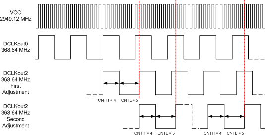
9.3.3.3 Single and Multiple Dynamic Digital Delay Example
In this example, two separate adjustments are made to the device clocks. In the first adjustment, a single delay of 1 VCO cycle occurs between DCLKout2 and DCLKout0. In the second adjustment, two delays of 1 VCO cycle occur between DCLKout2 and DCLKout0. At this point in the example, DCLKout2 is delayed 3 VCO cycles behind DCLKout0.
Assuming the device already has the following initial configurations:
- VCO frequency: 2949.12 MHz
- DCLKout0 = 368.64 MHz, DCLKout0_DIV = 8
- DCLKout2 = 368.64 MHz, DCLKout2_DIV = 8
The following steps illustrate the example above:
- Set DCLKout2_DDLY_CNTH = 4. First part of delay for DCLKout2.
- Set DCLKout2_DDLY_CNTL = 5. Second part of delay for DCLKout2.
- Set DCLKout2_DDLY_PD = 0. Enable the digital delay for DCLKout2.
- Set DDLYd2_EN = 1. Enable dynamic digital delay for DCLKout2.
- Set SYNC_DIS0 = 1 and SYNC_DIS2 = 0. Sync should be disabled to DCLKout0, but not DCLKout2.
- Set SYNC_MODE = 3. Enable SYNC event from SPI write to the DDLYd_STEP_CNT register.
- Set SYNC_MODE = 2, SYSREF_MUX = 2. Setup proper SYNC settings.
- Set DDLYd_STEP_CNT = 1. This begins the first adjustment.
- Set DDLYd_STEP_CNT = 2. This begins the second adjustment.
Before step 8 DCLKout2 clock edge is aligned with DCLKout0.
After step 8, DCLKout2 counts four VCO cycles high and then five VCO cycles low as programmed by DCLKout2_DDLY_CNTH and DCLKout2_DDLY_CNTL fields, effectively delaying DCLKout2 by one VCO cycle with respect to DCLKout0. This is the first adjustment.
Before step 9, DCLKout2 clock edge was delayed 1 VCO cycle from DCLKout0.
After step 9, DCLKout2 counts four VCO cycles high and then five VCO cycles low, as programmed by DCLKout2_DDLY_CNTH and DCLKout2_DDLY_CNTL fields twice, delaying DCLKout2 by two VCO cycles with respect to DCLKout0. This is the second adjustment.
 Figure 15. Single and Multiple Adjustment Dynamic Digital Delay Example