SNOSDB6C December 2020 – March 2022 LMP7704-SP
PRODUCTION DATA
- 1 Features
- 2 Applications
- 3 Description
- 4 Revision History
- 5 Pin Configuration and Functions
- 6 Specifications
- 7 Detailed Description
- 8 Application and Implementation
- 9 Power Supply Recommendations
- 10Layout
- 11Device and Documentation Support
- 12Mechanical, Packaging, and Orderable Information
Package Options
Mechanical Data (Package|Pins)
- HBH|14
Thermal pad, mechanical data (Package|Pins)
Orderable Information
8.1.1 Low Input Voltage Noise
The LMP7704-SP has a very low input voltage noise of 9 nV/√Hz. This input voltage noise is further reduced by placing N amplifiers in parallel, as shown in Figure 8-1. The total voltage noise on the output of this circuit is divided by the square root of the number of amplifiers used in this parallel combination. The reason is because each individual amplifier acts as an independent noise source, and the average noise of independent sources is the quadrature sum of the independent sources divided by the number of sources. For N identical amplifiers:
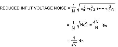
Figure 8-1 shows a schematic of this input voltage noise reduction circuit. Typical resistor values are:
RG = 10 Ω, RF = 1 kΩ, and RO = 1 kΩ.
 Figure 8-1 Noise Reduction Circuit