SNAS521H July   2011  – January 2016 LMP90077 , LMP90078 , LMP90079 , LMP90080

PRODUCTION DATA.  

  1. Features
  2. Applications
  3. Description
  4. Revision History
  5. Description (continued)
  6. Device Comparison Table
  7. Pin Configuration and Functions
  8. Specifications
    1. 8.1  Absolute Maximum Ratings
    2. 8.2  ESD Ratings
    3. 8.3  Recommended Operating Conditions
    4. 8.4  Thermal Information
    5. 8.5  Electrical Characteristics
    6. 8.6  Timing Requirements
    7. 8.7  Timing Requirements - CSB Timing
    8. 8.8  Timing Requirements - SCLK and SDI Timing
    9. 8.9  Timing Requirements - SDO Timing With DOD1
    10. 8.10 Timing Requirements - SDO Timing with DOD2
    11. 8.11 Timing Requirements - SDO and DRDYB Timing
    12. 8.12 Typical Characteristics
  9. Detailed Description
    1. 9.1 Overview
    2. 9.2 Functional Block Diagram
    3. 9.3 Feature Description
      1. 9.3.1 Calibration
        1. 9.3.1.1 Background Calibration
          1. 9.3.1.1.1 Types of Background Calibration:
          2. 9.3.1.1.2 Using Background Calibration:
        2. 9.3.1.2 System Calibration
          1. 9.3.1.2.1 System Calibration Offset Coefficient Determination Mode
          2. 9.3.1.2.2 System Calibration Gain Coefficient Determination Mode
          3. 9.3.1.2.3 Post-Calibration Scaling
      2. 9.3.2 True Continuous Background Calibration
      3. 9.3.3 Continuous Background Sensor Diagnostics
      4. 9.3.4 Flexible Input MUX Channels
      5. 9.3.5 Programmable Gain Amplifiers (FGA & PGA)
      6. 9.3.6 Excitation Current Sources (IB1 & IB2) - LMP90080/LMP90078
      7. 9.3.7 Signal Path
        1. 9.3.7.1 Reference Input (VREF)
        2. 9.3.7.2 Flexible Input MUX (VIN)
        3. 9.3.7.3 Selectable Gains (FGA and PGA)
        4. 9.3.7.4 Buffer (BUFF)
        5. 9.3.7.5 Internal/External CLK Selection
        6. 9.3.7.6 Programmable ODRS
        7. 9.3.7.7 Digital Filter
        8. 9.3.7.8 GPIO (D0-D6)
    4. 9.4 Device Functional Modes
      1. 9.4.1 Channels Scan Mode
        1. 9.4.1.1 ScanMode0: Single-Channel Continuous Conversion
        2. 9.4.1.2 ScanMode1: Multiple-Channels Single Scan
        3. 9.4.1.3 ScanMode2: Multiple-Channels Continuous Scan
        4. 9.4.1.4 ScanMode3: Multiple-Channels Continuous Scan with Burnout Currents
      2. 9.4.2 Sensor Interface
        1. 9.4.2.1 IB1 & IB2 - Excitation Currents (LMP90080/LMP90078)
        2. 9.4.2.2 Burnout Currents
          1. 9.4.2.2.1 Burnout Current Injection
        3. 9.4.2.3 Sensor Diagnostic Flags
          1. 9.4.2.3.1 SHORT_THLD_FLAG
          2. 9.4.2.3.2 RAILS_FLAG
          3. 9.4.2.3.3 POR_AFT_LST_RD
          4. 9.4.2.3.4 OFLO_FLAGS
          5. 9.4.2.3.5 SAMPLED_CH
    5. 9.5 Programming
      1. 9.5.1 Serial Digital Interface
        1. 9.5.1.1 Register Address (ADDR)
        2. 9.5.1.2 Register Read/Write Protocol
        3. 9.5.1.3 Streaming
        4. 9.5.1.4 CSB - Chip Select Bar
        5. 9.5.1.5 SPI Reset
        6. 9.5.1.6 DRDYB - Data Ready Bar
          1. 9.5.1.6.1 DrdybCase1: Combining SDO/DRDYB with SDO_DRDYB_DRIVER = 0x00
          2. 9.5.1.6.2 DrdybCase2: Combining SDO/DRDYB with SDO_DRDYB_DRIVER = 0x03
          3. 9.5.1.6.3 DrdybCase3: Routing DRDYB to D6
        7. 9.5.1.7 Data Only Read Transaction
        8. 9.5.1.8 Cyclic Redundancy Check (CRC)
      2. 9.5.2 RESET and RESTART
      3. 9.5.3 Register Read/Write Examples
        1. 9.5.3.1 Writing to Register Examples
        2. 9.5.3.2 Reading from Register Example
      4. 9.5.4 Streaming Examples
        1. 9.5.4.1 Normal Streaming Example
        2. 9.5.4.2 Controlled Streaming Example
    6. 9.6 Register Maps
      1. 9.6.1 Power and Reset Registers
      2. 9.6.2 ADC Registers
      3. 9.6.3 Channel Configuration Registers  
      4. 9.6.4 Calibration Registers
      5. 9.6.5 Sensor Diagnostic Registers
      6. 9.6.6 SPI Registers
      7. 9.6.7 GPIO Registers
  10. 10Application and Implementation
    1. 10.1 Application Information
      1. 10.1.1 Connecting the Supplies
        1. 10.1.1.1 VA and VIO
        2. 10.1.1.2 VREF
      2. 10.1.2 Quick Start
      3. 10.1.3 ADC_DOUT Calculation
    2. 10.2 Typical Applications
      1. 10.2.1 Typical Sensor Application
        1. 10.2.1.1 Design Requirements
        2. 10.2.1.2 Detailed Design Procedure
        3. 10.2.1.3 Application Curve
      2. 10.2.2 3-Wire RTD
        1. 10.2.2.1 Design Requirements
        2. 10.2.2.2 Detailed Design Procedure
        3. 10.2.2.3 Application Curve
      3. 10.2.3 Thermocouple and IC Analog Temperature
        1. 10.2.3.1 Design Requirements
        2. 10.2.3.2 Detailed Design Procedure
        3. 10.2.3.3 Application Curve
  11. 11Power Supply Recommendations
  12. 12Layout
    1. 12.1 Layout Guidelines
    2. 12.2 Layout Example
  13. 13Device and Documentation Support
    1. 13.1 Device Support
      1. 13.1.1 Device Nomenclature
    2. 13.2 Related Links
    3. 13.3 Community Resources
    4. 13.4 Trademarks
    5. 13.5 Electrostatic Discharge Caution
    6. 13.6 Glossary
  14. 14Mechanical, Packaging, and Orderable Information

Package Options

Mechanical Data (Package|Pins)
Thermal pad, mechanical data (Package|Pins)
Orderable Information

11 Power Supply Recommendations

The device can be placed in Active, Power-Down, or Stand-By state.

In Power-Down, the ADC is not converting data, contents of the registers are unaffected, and there is a drastic power reduction. In Stand-By, the ADC is not converting data, but the power is only slightly reduced so that the device can quickly transition into the active state if desired.

These states can be selected using the PWRCN register. When written, PWRCN brings the device into the Active, Power-Down, or Stand-By state. When read, PWRCN indicates the state of the device.

The read value would confirm the write value after a small latency (approximately 15 µs with the internal CLK). It may be appropriate to wait for this latency to confirm the state change. Requests not adhering to this latency requirement may be rejected.

It is not possible to make a direct transition from the power-down state to the stand-by state. This state diagram is shown below.
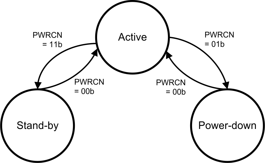
LMP90077 LMP90078 LMP90079 LMP90080 30169788.gif Figure 79. Active, Power-Down, Stand-By State Diagram