SNVS737F October 2011 – June 2019 LMR24220
PRODUCTION DATA.
- 1 Features
- 2 Applications
- 3 Description
- 4 Revision History
- 5 Pin Configuration and Functions
- 6 Specifications
- 7 Detailed Description
- 8 Application and Implementation
- 9 Layout
- 10Device and Documentation Support
- 11Mechanical, Packaging, and Orderable Information
Package Options
Mechanical Data (Package|Pins)
- YPA|28
Thermal pad, mechanical data (Package|Pins)
Orderable Information
5 Pin Configuration and Functions
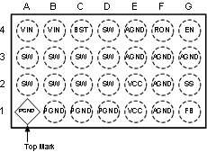
YPA Package
28-Bump DSGBA
Top View

Pin Descriptions
| PIN | DESCRIPTION | ||
|---|---|---|---|
| NO. | NAME | ||
| A2, A3, B2, B3, C2, C3, D2, D3, D4 | SW | Switching node | Internally connected to the source of the main MOSFET and the drain of the synchronous MOSFET. Connect to the inductor. |
| A4, B4 | VIN | Input supply voltage | Supply pin to the device. Nominal input range is 4.5 V to 42 V. |
| C4 | BST | Connection for bootstrap capacitor | Connect a 33-nF capacitor from the SW pin to this pin. An internal diode charges the capacitor during the main MOSFET off-time. |
| E3, E4, F1, F2, F3, G3 | AGND | Analog Ground | Ground for all internal circuitry other than the PGND pin. |
| G2 | SS | Soft start | An 8-µA internal current source charges an external capacitor to provide the soft- start function. |
| G1 | FB | Feedback | Internally connected to the regulation and over-voltage comparators. The regulation setting is 0.8V at this pin. Connect to feedback resistors. |
| G4 | EN | Enable | Connect a voltage higher than 1.26 V to enable the regulator. Leaving this input open circuit will enable the device at internal UVLO level. |
| F4 | RON | On-time control | An external resistor from the VIN pin to this pin sets the main MOSFET on-time. |
| E1, E2 | VCC | Start-up regulator Output | Nominally regulated to 6 V. Connect a capacitor of not less than 680 nF between the VCC and AGND pins for stable operation. |
| A1, B1, C1, D1 | PGND | Power ground | Synchronous MOSFET source connection. Tie to a ground plane. |