SNVS737F October   2011  – June 2019 LMR24220

PRODUCTION DATA.  

  1. Features
  2. Applications
  3. Description
    1.     Device Images
      1.      Typical Application
  4. Revision History
  5. Pin Configuration and Functions
    1.     Pin Descriptions
  6. Specifications
    1. 6.1 Absolute Maximum Ratings
    2. 6.2 Recommended Operating Ratings
    3. 6.3 Electrical Characteristics
    4. 6.4 Typical Characteristics
  7. Detailed Description
    1. 7.1 Overview
    2. 7.2 Functional Block Diagram
    3. 7.3 Feature Description
      1. 7.3.1  CoT Control Circuit Overview
      2. 7.3.2  Start-up Regulator (VCC)
      3. 7.3.3  Regulation Comparator
      4. 7.3.4  Zero Coil Current Detect
      5. 7.3.5  Overvoltage Comparator
      6. 7.3.6  On-Time Timer, Shutdown
      7. 7.3.7  Current Limit
      8. 7.3.8  N-Channel MOSFET and Driver
      9. 7.3.9  Soft Start
      10. 7.3.10 Thermal Protection
  8. Application and Implementation
    1. 8.1 Application Information
    2. 8.2 Typical Application
      1. 8.2.1 Detailed Design Procedure
        1. 8.2.1.1 Custom Design With WEBENCH® Tools
        2. 8.2.1.2 External Components
      2. 8.2.2 Application Curve
  9. Layout
    1. 9.1 Layout Guidelines
    2. 9.2 Package Considerations
    3. 9.3 Thermal Derating
  10. 10Device and Documentation Support
    1. 10.1 Device Support
      1. 10.1.1 Development Support
        1. 10.1.1.1 Custom Design With WEBENCH® Tools
    2. 10.2 Receiving Notification of Documentation Updates
    3. 10.3 Community Resources
    4. 10.4 Trademarks
    5. 10.5 Electrostatic Discharge Caution
    6. 10.6 Glossary
  11. 11Mechanical, Packaging, and Orderable Information

Package Options

Mechanical Data (Package|Pins)
Thermal pad, mechanical data (Package|Pins)
Orderable Information

Thermal Derating

Temperature rise increases with frequency, load current, input voltage and smaller board dimensions. On a typical board, the LMR24220 is capable of supplying 2 A below an ambient temperature of 50°C under worst case operation with input voltage of 42 V. Figure 27 shows a thermal derating curve for the output current without thermal shutdown against ambient temperature up to 125°C. Obtaining 2-A output current is possible at higher temperature by increasing the PCB ground plane area, adding air flow or reducing the input voltage or operating frequency
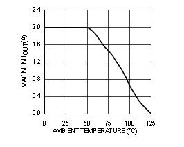
LMR24220 30167674.gif
θJA = 40°C/W, VOUT = 3.3 V, ƒSW = 500 kHz
(tested on the evaluation board)
Figure 27. Thermal Derating Curve