SNVSAN3F August 2017 – November 2020 LMR33630
PRODUCTION DATA
- 1
- 1 Features
- 2 Applications
- 3 Description
- 4 Revision History
- 5 Device Comparison Table
- 6 Pin Configuration and Functions
- 7 Specifications
- 8 Detailed Description
-
9 Application and Implementation
- 9.1 Application Information
- 9.2
Typical Application
- 9.2.1 Design Requirements
- 9.2.2
Detailed Design Procedure
- 9.2.2.1 Custom Design With WEBENCH® Tools
- 9.2.2.2 Choosing the Switching Frequency
- 9.2.2.3 Setting the Output Voltage
- 9.2.2.4 Inductor Selection
- 9.2.2.5 Output Capacitor Selection
- 9.2.2.6 Input Capacitor Selection
- 9.2.2.7 CBOOT
- 9.2.2.8 VCC
- 9.2.2.9 CFF Selection
- 9.2.2.10 External UVLO
- 9.2.2.11 Maximum Ambient Temperature
- 9.2.3 Application Curves
- 9.3 What to Do and What Not to Do
- Power Supply Recommendations
- 10Layout
- 11Device and Documentation Support
- 12Mechanical, Packaging, and Orderable Information
Package Options
Refer to the PDF data sheet for device specific package drawings
Mechanical Data (Package|Pins)
- RNX|12
- DDA|8
Thermal pad, mechanical data (Package|Pins)
Orderable Information
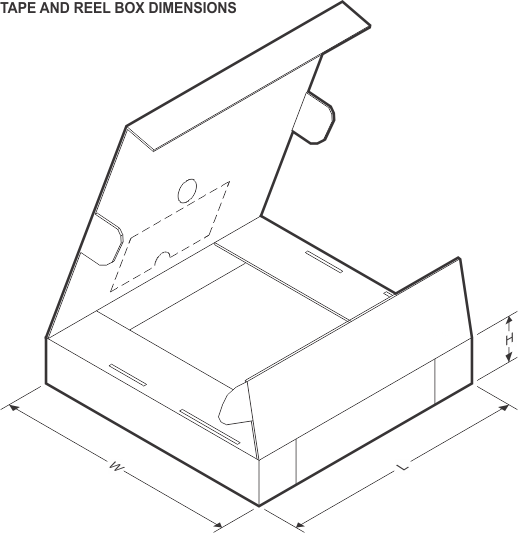
12.1 Tape and Reel Information

| Device | Package Type |
Package Drawing | Pins | SPQ | Reel Diameter (mm) |
Reel Width W1 (mm) |
A0 (mm) |
B0 (mm) |
K0 (mm) |
P1 (mm) |
W (mm) |
Pin1 Quadrant |
|---|---|---|---|---|---|---|---|---|---|---|---|---|
| LMR33630ADDAR | SO PowerPAD | DDA | 8 | 2500 | 330 | 12.4 | 6.4 | 5.2 | 2.1 | 8 | 12 | Q1 |
| LMR33630BDDAR | SO PowerPAD | DDA | 8 | 2500 | 330 | 12.4 | 6.4 | 5.2 | 2.1 | 8 | 12 | Q1 |
| LMR33630CDDAR | SO PowerPAD | DDA | 8 | 2500 | 330 | 12.4 | 6.4 | 5.2 | 2.1 | 8 | 12 | Q1 |
| Device | Package Type | Package Drawing | Pins | SPQ | Length (mm) | Width (mm) | Height (mm) |
|---|---|---|---|---|---|---|---|
| LMR33630ADDA | SO PowerPAD | DDA | 8 | 75 | 521 | 194 | 37 |
| LMR33630ADDAR | SO PowerPAD | DDA | 8 | 2500 | 353 | 353 | 36 |
| LMR33630BDDA | SO PowerPAD | DDA | 8 | 75 | 521 | 194 | 37 |
| LMR33630BDDAR | SO PowerPAD | DDA | 8 | 2500 | 353 | 353 | 36 |
| LMR33630CDDA | SO PowerPAD | DDA | 8 | 75 | 521 | 194 | 37 |
| LMR33630CDDAR | SO PowerPAD | DDA | 8 | 2500 | 353 | 353 | 36 |