SNVSBB4B December   2019  – November 2022 LMR36503

PRODUCTION DATA  

  1. Features
  2. Applications
  3. Description
  4. Revision History
  5. Device Comparison Table
  6. Pin Configuration and Functions
  7. Specifications
    1. 7.1 Absolute Maximum Ratings
    2. 7.2 ESD (Commercial) Ratings
    3. 7.3 Recommended Operating Conditions
    4. 7.4 Thermal Information
    5. 7.5 Electrical Characteristics
    6. 7.6 Timing Characteristics
    7. 7.7 Switching Characteristics
    8. 7.8 System Characteristics
    9. 7.9 Typical Characteristics
  8. Detailed Description
    1. 8.1 Overview
    2. 8.2 Functional Block Diagram
    3. 8.3 Feature Description
      1. 8.3.1  Enable, Start-up, and Shutdown
      2. 8.3.2  Adjustable Switching Frequency (with RT)
      3. 8.3.3  Power-Good Output Operation
      4. 8.3.4  Internal LDO, VCC UVLO, and VOUT/BIAS Input
      5. 8.3.5  Bootstrap Voltage and VCBOOT-UVLO (CBOOT Terminal)
      6. 8.3.6  Output Voltage Selection
      7. 8.3.7  Soft Start and Recovery from Dropout
        1. 8.3.7.1 Recovery from Dropout
      8. 8.3.8  Current Limit and Short Circuit
      9. 8.3.9  Thermal Shutdown
      10. 8.3.10 Input Supply Current
    4. 8.4 Device Functional Modes
      1. 8.4.1 Shutdown Mode
      2. 8.4.2 Standby Mode
      3. 8.4.3 Active Mode
        1. 8.4.3.1 CCM Mode
        2. 8.4.3.2 Auto Mode - Light Load Operation
          1. 8.4.3.2.1 Diode Emulation
          2. 8.4.3.2.2 Frequency Reduction
        3. 8.4.3.3 FPWM Mode - Light Load Operation
        4. 8.4.3.4 Minimum On-time (High Input Voltage) Operation
        5. 8.4.3.5 Dropout
  9. Application and Implementation
    1. 9.1 Application Information
    2. 9.2 Typical Application
      1. 9.2.1 Design Requirements
      2. 9.2.2 Detailed Design Procedure
        1. 9.2.2.1 Choosing the Switching Frequency
        2. 9.2.2.2 Setting the Output Voltage
          1. 9.2.2.2.1 FB for Adjustable Output
        3. 9.2.2.3 Inductor Selection
        4. 9.2.2.4 Output Capacitor Selection
        5. 9.2.2.5 Input Capacitor Selection
        6. 9.2.2.6 CBOOT
        7. 9.2.2.7 VCC
        8. 9.2.2.8 CFF Selection
          1. 9.2.2.8.1 External UVLO
        9. 9.2.2.9 Maximum Ambient Temperature
      3. 9.2.3 Application Curves
    3. 9.3 Best Design Practices
    4. 9.4 Power Supply Recommendations
    5. 9.5 Layout
      1. 9.5.1 Layout Guidelines
        1. 9.5.1.1 Ground and Thermal Considerations
      2. 9.5.2 Layout Example
  10. 10Device and Documentation Support
    1. 10.1 Documentation Support
      1. 10.1.1 Related Documentation
    2. 10.2 Receiving Notification of Documentation Updates
    3. 10.3 Support Resources
    4. 10.4 Trademarks
    5. 10.5 Electrostatic Discharge Caution
    6. 10.6 Glossary
  11. 11Mechanical, Packaging, and Orderable Information

Package Options

Mechanical Data (Package|Pins)
Thermal pad, mechanical data (Package|Pins)
Orderable Information

Application Curves

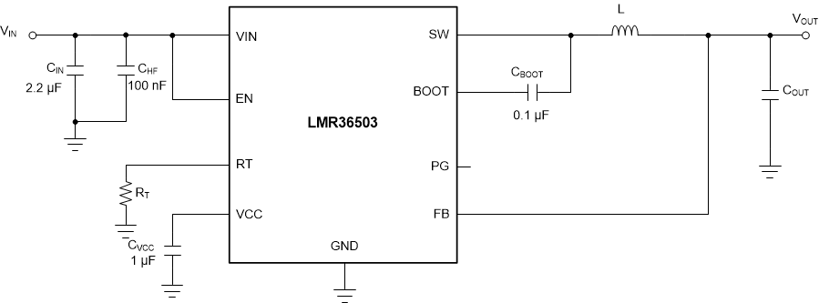
Unless otherwise specified the following conditions apply: VIN = 24V, TA = 25°C. Figure 9-16shows the circuit with the appropriate BOM in Table 9-3
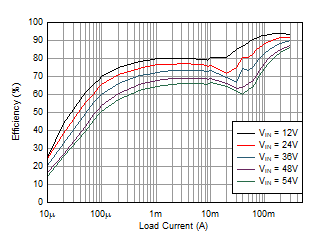
Unless otherwise specified the following conditions apply: VIN = 24V, TA = 25°C. Figure 9-16shows the circuit with the appropriate BOM in Table 9-3 GUID-20201209-CA0I-DX2N-TMFQ-N6N2K0TWJT1V-low.gif
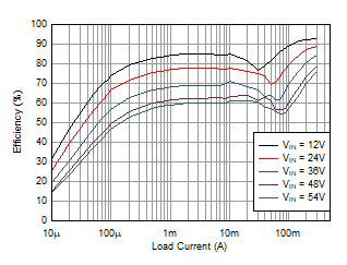
LMR36503R5 VOUT = 5 V Fixed 400 kHz (AUTO)
Figure 9-4 Efficiency. Unless otherwise specified the following conditions apply: VIN = 24V, TA = 25°C. Figure 9-16shows the circuit with the appropriate BOM in Table 9-3
GUID-20201209-CA0I-0PPV-DFT8-31WSD0ZDGVR2-low.gif
LMR36503R5 VOUT = 5 V Fixed 1 MHz (AUTO)
Figure 9-6 Efficiency
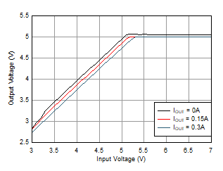
GUID-20201209-CA0I-L1XG-MRJK-KT2DV11PNZDT-low.gif
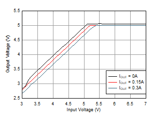
LMR36503R5 VOUT = 5 V Fixed 400 kHz (AUTO)
Figure 9-8 Dropout
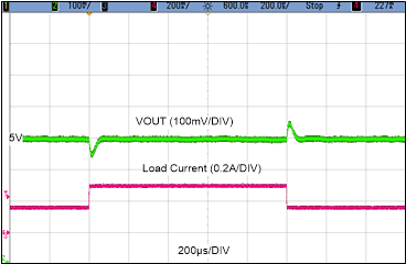
GUID-20201209-CA0I-RRMW-NK9M-ZW7CRC6ZHKWJ-low.gif
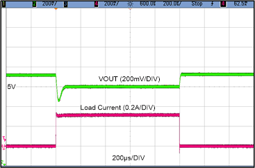
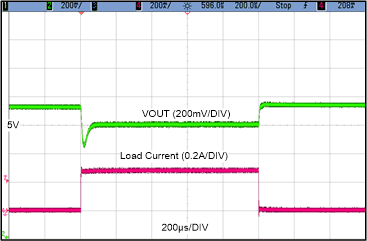
LMR36503R5 VOUT = 5 V Fixed 400 kHz
0 A to 0.3 A,1 A/µs
Figure 9-10 Load Transient
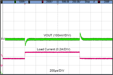
GUID-20201209-CA0I-TN2S-PV1F-QD8GZC0DDWT4-low.gif
LMR36503R5 VOUT = 5 V Fixed 1 MHz
0 A to 0.3 A,1 A/µs
Figure 9-12 Load Transient
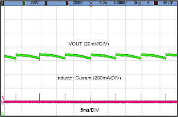
GUID-20201209-CA0I-GZMK-6FBJ-5RL2NNFFQN58-low.gif
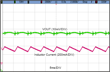
LMR36503R5 VOUT = 5 V Fixed 300 mA
Figure 9-14 Output Ripple
GUID-20201209-CA0I-T1TF-PGZQ-7C5DGP9SCD7D-low.gif
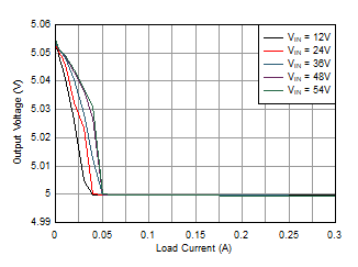
LMR36503R5 VOUT = 5 V Fixed 400 kHz (AUTO)
Figure 9-5 Line and Load Regulation
GUID-20201209-CA0I-FZC1-K7LD-RQ4FVBQPRNNC-low.gif
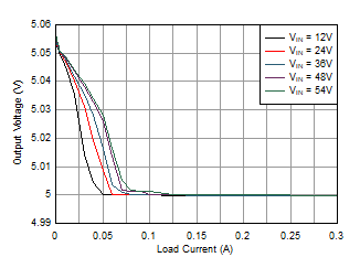
LMR36503R5 VOUT = 5 V Fixed 1 MHz (AUTO)
Figure 9-7 Line and Load Regulation
GUID-20201209-CA0I-XG13-GSKC-GLXFSWWMPLM6-low.gif
LMR36503R5 VOUT = 5 V Fixed 1 MHz (AUTO)
Figure 9-9 Dropout
GUID-20201209-CA0I-21HB-W8FK-GDHNLHB5T3N7-low.gif
LMR36503R5 VOUT = 5 V Fixed 400 kHz
0.15 A to 0.3 A,1 A/µs
Figure 9-11 Load Transient
GUID-20201209-CA0I-9MWN-SW0X-2TNDDQHJMFLM-low.gif
LMR36503R5 VOUT = 5 V Fixed 1 MHz
0.15 A to 0.3 A,1 A/µs
Figure 9-13 Load Transient
GUID-20201209-CA0I-PNN2-4CRS-8JBF52JSQHVB-low.gif
LMR36503R5 VOUT = 5 V Fixed No Load
Figure 9-15 Output Ripple
GUID-20201216-CA0I-VCKR-HCNL-FWQZHSLFNM4V-low.gif Figure 9-16 Schematic for Typical Application Curves
Table 9-3 BOM for Typical Application Curves
U1 ƒSW VOUT L NOMINAL COUT
(RATED CAPACITANCE)
RT pin
LMR36503R5RPER 400 kHz 5 V 100 µH, 380 mΩ 2 × 22 µF 39.2kΩ
LMR36503R5RPER 1 MHz 5 V 47 µH, 84 mΩ 1 × 22 µF Short to VCC