SNVSBB4B December 2019 – November 2022 LMR36503
PRODUCTION DATA
- 1 Features
- 2 Applications
- 3 Description
- 4 Revision History
- 5 Device Comparison Table
- 6 Pin Configuration and Functions
- 7 Specifications
-
8 Detailed Description
- 8.1 Overview
- 8.2 Functional Block Diagram
- 8.3
Feature Description
- 8.3.1 Enable, Start-up, and Shutdown
- 8.3.2 Adjustable Switching Frequency (with RT)
- 8.3.3 Power-Good Output Operation
- 8.3.4 Internal LDO, VCC UVLO, and VOUT/BIAS Input
- 8.3.5 Bootstrap Voltage and VCBOOT-UVLO (CBOOT Terminal)
- 8.3.6 Output Voltage Selection
- 8.3.7 Soft Start and Recovery from Dropout
- 8.3.8 Current Limit and Short Circuit
- 8.3.9 Thermal Shutdown
- 8.3.10 Input Supply Current
- 8.4 Device Functional Modes
-
9 Application and Implementation
- 9.1 Application Information
- 9.2
Typical Application
- 9.2.1 Design Requirements
- 9.2.2 Detailed Design Procedure
- 9.2.3 Application Curves
- 9.3 Best Design Practices
- 9.4 Power Supply Recommendations
- 9.5 Layout
- 10Device and Documentation Support
- 11Mechanical, Packaging, and Orderable Information
Package Options
Mechanical Data (Package|Pins)
- RPE|9
Thermal pad, mechanical data (Package|Pins)
- RPE|9
Orderable Information
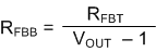
8.3.6 Output Voltage Selection
In the LMR36503 family, select variants with an adjustable output voltage option (see Section 5), and you need an external resistor divider connection between the output voltage node, the device FB pin, and the system GND, as shown in Figure 8-6. The variants with adjustable output voltage option in the LMR36503 family are designed with a 1-V internal reference voltage.
When using the fixed-output variants from the LMR36503 family, simply connect the FB pin is identified as VOUT/BIAS pin for fixed-output variants in the rest of the data sheet) to the system output voltage node. See Section 5 for more details.
 Figure 8-6 Setting Output Voltage for Adjustable Output Variant
In adjustable output voltage variants, an addition feed-forward capacitor, CFF, in parallel with the RFBT, can be used to optimize the phase margin and transient response. See Section 9.2.2.8 for more details. No additional resistor divider or feed-forward capacitor, CFF, is needed in fixed-output variants.