SNVSBB4B December   2019  – November 2022 LMR36503

PRODUCTION DATA  

  1. Features
  2. Applications
  3. Description
  4. Revision History
  5. Device Comparison Table
  6. Pin Configuration and Functions
  7. Specifications
    1. 7.1 Absolute Maximum Ratings
    2. 7.2 ESD (Commercial) Ratings
    3. 7.3 Recommended Operating Conditions
    4. 7.4 Thermal Information
    5. 7.5 Electrical Characteristics
    6. 7.6 Timing Characteristics
    7. 7.7 Switching Characteristics
    8. 7.8 System Characteristics
    9. 7.9 Typical Characteristics
  8. Detailed Description
    1. 8.1 Overview
    2. 8.2 Functional Block Diagram
    3. 8.3 Feature Description
      1. 8.3.1  Enable, Start-up, and Shutdown
      2. 8.3.2  Adjustable Switching Frequency (with RT)
      3. 8.3.3  Power-Good Output Operation
      4. 8.3.4  Internal LDO, VCC UVLO, and VOUT/BIAS Input
      5. 8.3.5  Bootstrap Voltage and VCBOOT-UVLO (CBOOT Terminal)
      6. 8.3.6  Output Voltage Selection
      7. 8.3.7  Soft Start and Recovery from Dropout
        1. 8.3.7.1 Recovery from Dropout
      8. 8.3.8  Current Limit and Short Circuit
      9. 8.3.9  Thermal Shutdown
      10. 8.3.10 Input Supply Current
    4. 8.4 Device Functional Modes
      1. 8.4.1 Shutdown Mode
      2. 8.4.2 Standby Mode
      3. 8.4.3 Active Mode
        1. 8.4.3.1 CCM Mode
        2. 8.4.3.2 Auto Mode - Light Load Operation
          1. 8.4.3.2.1 Diode Emulation
          2. 8.4.3.2.2 Frequency Reduction
        3. 8.4.3.3 FPWM Mode - Light Load Operation
        4. 8.4.3.4 Minimum On-time (High Input Voltage) Operation
        5. 8.4.3.5 Dropout
  9. Application and Implementation
    1. 9.1 Application Information
    2. 9.2 Typical Application
      1. 9.2.1 Design Requirements
      2. 9.2.2 Detailed Design Procedure
        1. 9.2.2.1 Choosing the Switching Frequency
        2. 9.2.2.2 Setting the Output Voltage
          1. 9.2.2.2.1 FB for Adjustable Output
        3. 9.2.2.3 Inductor Selection
        4. 9.2.2.4 Output Capacitor Selection
        5. 9.2.2.5 Input Capacitor Selection
        6. 9.2.2.6 CBOOT
        7. 9.2.2.7 VCC
        8. 9.2.2.8 CFF Selection
          1. 9.2.2.8.1 External UVLO
        9. 9.2.2.9 Maximum Ambient Temperature
      3. 9.2.3 Application Curves
    3. 9.3 Best Design Practices
    4. 9.4 Power Supply Recommendations
    5. 9.5 Layout
      1. 9.5.1 Layout Guidelines
        1. 9.5.1.1 Ground and Thermal Considerations
      2. 9.5.2 Layout Example
  10. 10Device and Documentation Support
    1. 10.1 Documentation Support
      1. 10.1.1 Related Documentation
    2. 10.2 Receiving Notification of Documentation Updates
    3. 10.3 Support Resources
    4. 10.4 Trademarks
    5. 10.5 Electrostatic Discharge Caution
    6. 10.6 Glossary
  11. 11Mechanical, Packaging, and Orderable Information

Package Options

Mechanical Data (Package|Pins)
Thermal pad, mechanical data (Package|Pins)
Orderable Information
Diode Emulation

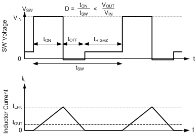
Diode emulation prevents reverse current through the inductor which requires a lower frequency needed to regulate given a fixed peak inductor current. Diode emulation also limits ripple current as frequency is reduced. With a fixed peak current, as output current is reduced to zero, frequency must be reduced to near zero to maintain regulation.
GUID-FF99B2E3-3E13-4E51-818C-D32D965A8332-low.gif
In auto mode, the low-side device is turned off after SW node current is near zero. As a result, after output current is less than half of what inductor ripple is in CCM, the part operates in DCM which is equivalent to the statement that diode emulation is active.
Figure 8-15 PFM Operation

The LMR36503 has a minimum peak inductor current setting (ILPK (see IPEAK-MIN in Section 7.5) while in auto mode. After current is reduced to a low value with fixed input voltage, on-time is constant. Regulation is then achieved by adjusting frequency. This mode of operation is called PFM mode regulation.