SLUSEG8D October   2021  – April 2024 LMR54406 , LMR54410

PRODUCTION DATA  

  1.   1
  2. Features
  3. Applications
  4. Description
  5. Device Comparison Table
  6. Pin Configuration and Functions
  7. Specifications
    1. 6.1 Absolute Maximum Ratings
    2. 6.2 ESD Ratings
    3. 6.3 Recommended Operating Conditions
    4. 6.4 Thermal Information
    5. 6.5 Electrical Characteristics
    6. 6.6 Timing Requirements
    7. 6.7 System Characteristics
    8. 6.8 Typical Characteristics
  8. Detailed Description
    1. 7.1 Overview
    2. 7.2 Functional Block Diagram
    3. 7.3 Feature Description
      1. 7.3.1 Fixed Frequency Peak Current Mode Control
      2. 7.3.2 Adjustable Output Voltage
      3. 7.3.3 Enable
      4. 7.3.4 Minimum ON Time, Minimum OFF Time, and Frequency Foldback
      5. 7.3.5 Bootstrap Voltage
      6. 7.3.6 Overcurrent and Short Circuit Protection
      7. 7.3.7 Soft Start
      8. 7.3.8 Thermal Shutdown
    4. 7.4 Device Functional Modes
      1. 7.4.1 Shutdown Mode
      2. 7.4.2 Active Mode
      3. 7.4.3 CCM Mode
      4. 7.4.4 Light Load Operation (PFM Version)
      5. 7.4.5 Light-Load Operation (FPWM Version)
  9. Application and Implementation
    1. 8.1 Application Information
    2. 8.2 Typical Application
      1. 8.2.1 Design Requirements
      2. 8.2.2 Detailed Design Procedure
        1. 8.2.2.1 Output Voltage Set-Point
        2. 8.2.2.2 Switching Frequency
        3. 8.2.2.3 Inductor Selection
        4. 8.2.2.4 Output Capacitor Selection
        5. 8.2.2.5 Input Capacitor Selection
        6. 8.2.2.6 Bootstrap Capacitor
        7. 8.2.2.7 Undervoltage Lockout Set-Point
        8. 8.2.2.8 Replacing Non Sync Converter
      3. 8.2.3 Application Curves
    3. 8.3 Power Supply Recommendations
    4. 8.4 Layout
      1. 8.4.1 Layout Guidelines
        1. 8.4.1.1 Compact Layout for EMI Reduction
        2. 8.4.1.2 Feedback Resistors
      2. 8.4.2 Layout Example
  10. Device and Documentation Support
    1. 9.1 Device Support
      1. 9.1.1 Third-Party Products Disclaimer
    2. 9.2 Documentation Support
      1. 9.2.1 Related Documentation
    3. 9.3 Receiving Notification of Documentation Updates
    4. 9.4 Support Resources
    5. 9.5 Trademarks
    6. 9.6 Electrostatic Discharge Caution
    7. 9.7 Glossary
  11. 10Revision History
  12. 11Mechanical, Packaging, and Orderable Information

Package Options

Mechanical Data (Package|Pins)
Thermal pad, mechanical data (Package|Pins)
Orderable Information

Description

The LMR544xx is a wide-VIN, easy-to-use synchronous buck converter capable of driving up to 1A and 0.6A load current. With a wide input range of 4V to 36V, the device is designed for a wide range of industrial applications for power conditioning from an unregulated source.

The LMR544xx operates at 1.1MHz switching frequency to support use of relatively small inductors for an optimized design size. The devices have a PFM version to realize high efficiency at light load and a FPWM version to achieve constant frequency and small output voltage ripple over the full load range. Soft-start and compensation circuits are implemented internally, which allow the device to be used with minimal external components.

The device has built-in protection features, such as cycle-by-cycle current limit, hiccup mode short-circuit protection, and thermal shutdown in case of excessive power dissipation.

Device Information
PART NUMBER(3)PACKAGE(1)PACKAGE SIZE(2)
LMR54410DBV (SOT-23, 6)2.90mm × 2.80mm
LMR54406
For more information, see Section 11.
The package size (length × width) is a nominal value and includes pins, where applicable.
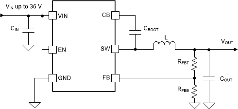
GUID-FE4A0CA2-50A1-43E6-B5CD-5B8B6AC6E250-low.gifSimplified Schematic
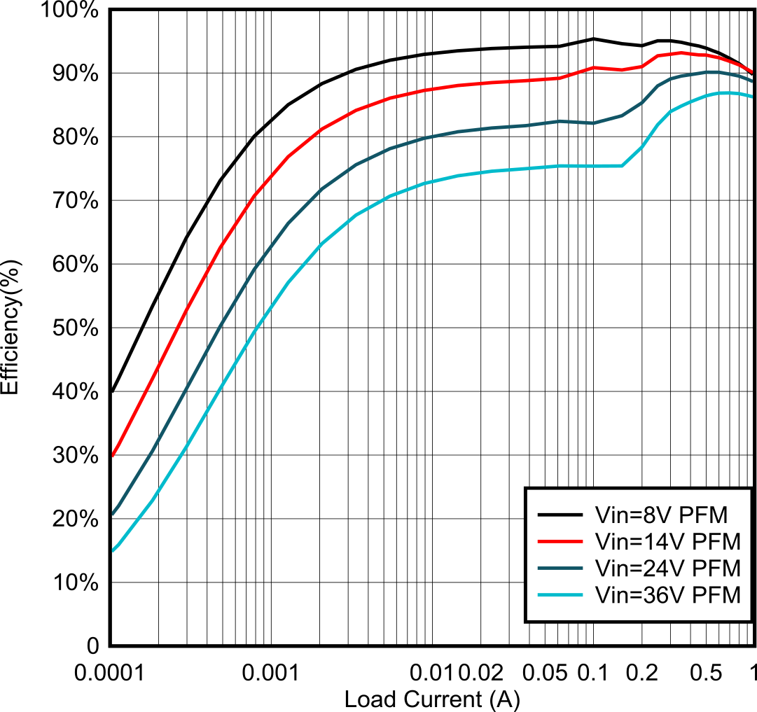
GUID-20211116-SS0I-QMPV-RNCZ-RV6HR21BZ2GB-low.pngEfficiency Versus Output Current;
VOUT = 5V, 1100kHz