SNWS018D December 2006 – June 2016 LMV221
PRODUCTION DATA.
- 1 Features
- 2 Applications
- 3 Description
- 4 Revision History
- 5 Pin Configuration and Functions
- 6 Specifications
- 7 Detailed Description
- 8 Application and Implementation
- 9 Power Supply Recommendations
- 10Layout
- 11Device and Documentation Support
- 12Mechanical, Packaging, and Orderable Information
Package Options
Mechanical Data (Package|Pins)
- NGF|6
Thermal pad, mechanical data (Package|Pins)
Orderable Information
1 Features
- 2.7-V to 3.3-V Supply Voltage
- 40-dB Linear in dB Power Detection Range
- 0.3-V to 2-V Output Voltage Range
- Shutdown
- Multi-Band Operation from 50 MHz to 3.5 GHz
- 0.5-dB Accurate Temperature Compensation
- External Configurable Output Filter Bandwidth
- 2.5 mm × 2.2 mm × 0.8 mm 6-pin WSON Package
2 Applications
- UMTS/CDMA/WCDMA RF Power Control
- GSM/GPRS RF Power Control
- PA Modules
- IEEE 802.11b, g (WLAN)
3 Description
The LMV221 is a 40-dB RF power detector intended for use in CDMA and WCDMA applications. The device has an RF frequency range from 50 MHz to 3.5 GHz. It provides an accurate temperature and supply-compensated output voltage that relates linearly to the RF input power in dBm. The circuit operates with a single supply from 2.7 V to 3.3 V.
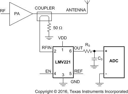
The LMV221 has an RF power detection range from −45 dBm to −5 dBm and is ideally suited for direct use in combination with a 30-dB directional coupler. Additional low-pass filtering of the output signal can be achieved by means of an external resistor and capacitor. Typical Application: Output RC Low Pass Filter shows a detector with an additional output low pass filter. The filter frequency is set with RS and CS.
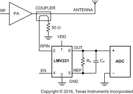
Typical Application: Feedback (R)C Low Pass Filter shows a detector with an additional feedback low pass filter. Resistor RP is optional and lowers the trans-impedance gain (RTRANS). The filter frequency is set with CP//CTRANS and RP//RTRANS.
The device is active for Enable = High, otherwise it is in a low power consumption shutdown mode. To save power and prevent discharge of an external filter capacitance, the output (OUT) is high-impedance during shutdown.
Device Information(1)
| PART NUMBER | PACKAGE | BODY SIZE (NOM) |
|---|---|---|
| LMV221 | WSON (6) | 2.50 mm × 2.20 mm |
space
space
space
Typical Application: Output RC Low Pass Filter

Typical Application: Feedback (R)C Low Pass Filter
