SNWS018D December 2006 – June 2016 LMV221
PRODUCTION DATA.
- 1 Features
- 2 Applications
- 3 Description
- 4 Revision History
- 5 Pin Configuration and Functions
- 6 Specifications
- 7 Detailed Description
- 8 Application and Implementation
- 9 Power Supply Recommendations
- 10Layout
- 11Device and Documentation Support
- 12Mechanical, Packaging, and Orderable Information
Package Options
Mechanical Data (Package|Pins)
- NGF|6
Thermal pad, mechanical data (Package|Pins)
Orderable Information
8 Application and Implementation
NOTE
Information in the following applications sections is not part of the TI component specification, and TI does not warrant its accuracy or completeness. TI’s customers are responsible for determining suitability of components for their purposes. Customers should validate and test their design implementation to confirm system functionality.
8.1 Application Information
8.1.1 Functionality and Applications of RF Power Detectors
8.1.1.1 Functionality of RF Power Detectors
An RF power detector is a device that produces a DC output voltage in response to the RF power level of the signal applied to its input. A wide variety of power detectors can be distinguished, each having certain properties that suit a particular application. This section provides an overview of the key characteristics of power detectors, and discusses the most important types of power detectors. The functional behavior of the LMV221 is discussed in detail.
8.1.1.1.1 Key Characteristics of RF Power Detectors
Power detectors are used to accurately measure the power of a signal inside the application. The attainable accuracy of the measurement is therefore dependent upon the accuracy and predictability of the detector transfer function from the RF input power to the DC output voltage.
Certain key characteristics determine the accuracy of RF detectors and they are classified accordingly:
- Temperature Stability
- Dynamic Range
- Waveform Dependency
- Transfer Shape
Generally, the transfer function of RF power detectors is slightly temperature dependent. This temperature drift reduces the accuracy of the power measurement, because most applications are calibrated at room temperature. In such systems, the temperature drift significantly contributes to the overall system power measurement error. The temperature stability of the transfer function differs for the various types of power detectors. Generally, power detectors that contain only one or few semiconductor devices (diodes, transistors) operating at RF frequencies attain the best temperature stability.
The dynamic range of a power detector is the input power range for which it creates an accurately reproducible output signal. What is considered accurate is determined by the applied criterion for the detector accuracy; the detector dynamic range is thus always associated with certain power measurement accuracy. This accuracy is usually expressed as the deviation of its transfer function from a certain predefined relationship, such as linear in dB for LOG detectors and square-law transfer (from input RF voltage to DC output voltage) for mean-square detectors. For LOG-detectors, the dynamic range is often specified as the power range for which its transfer function follows the ideal linear-in-dB relationship with an error smaller than or equal to ±1 dB. Again, the attainable dynamic range differs considerably for the various types of power detectors.
According to its definition, the average power is a metric for the average energy content of a signal and is not directly a function of the shape of the signal in time. In other words, the power contained in a 0-dBm sine wave is identical to the power contained in a 0-dBm square wave or a 0-dBm WCDMA signal; all these signals have the same average power. Depending on the internal detection mechanism, though, power detectors may produce a slightly different output signal in response to the aforementioned waveforms, even though their average power level is the same. This is due to the fact that not all power detectors strictly implement the definition formula for signal power, being the mean of the square of the signal. Most types of detectors perform some mixture of peak detection and average power detection. A waveform independent detector response is often desired in applications that exhibit a large variety of waveforms, such that separate calibration for each waveform becomes impractical.
The shape of the detector transfer function from the RF input power to the DC output voltage determines the required resolution of the ADC connected to it. The overall power measurement error is the combination of the error introduced by the detector, and the quantization error contributed by the ADC. The impact of the quantization error on the overall transfer's accuracy is highly dependent on the detector transfer shape, as shown in Figure 71 and Figure 72.
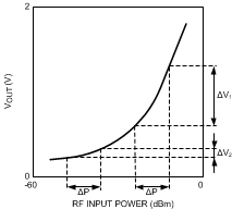
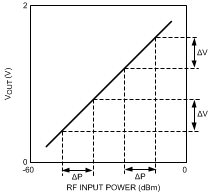
Figure 71 and Figure 72 shows two different representations of the detector transfer function. In both Figure 71 and Figure 72 the input power along the horizontal axis is displayed in dBm because most applications specify power accuracy requirements in dBm (or dB). Figure 71 shows a convex detector transfer function, while the transfer function on the right hand side is linear (in dB). The slope of the detector transfer function — the detector conversion gain – is of key importance for the impact of the quantization error on the total measurement error. If the detector transfer function slope is low, a change, ΔP, in the input power results only in a small change of the detector output voltage, such that the quantization error is relatively large. On the other hand, if the detector transfer function slope is high, the output voltage change for the same input power change will be large, such that the quantization error is small. Figure 72 has a very low slope at low input power levels, resulting in a relatively large quantization error. Therefore, to achieve accurate power measurement in this region, a high-resolution ADC is required. On the other hand, for high input power levels the quantization error are very small due to the steep slope of the curve in this region. For accurate power measurement in this region, a much lower ADC resolution is sufficient. Figure 71 has a constant slope over the power range of interest, such that the required ADC resolution for a certain measurement accuracy is constant. For this reason, the LOG-linear curve in Figure 71 generally leads to the lowest ADC resolution requirements for certain power measurement accuracy.
8.1.1.1.2 Types of RF Power Detectors
Three different detector types are distinguished based on the four characteristics previously discussed:
8.1.1.1.2.1 Diode Detector
A diode is one of the simplest types of RF detectors. As depicted in Figure 73, the diode converts the RF input voltage into a rectified current. This unidirectional current charges the capacitor. The RC time constant of the resistor and the capacitor determines the amount of filtering applied to the rectified (detected) signal.
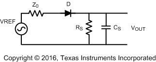 Figure 73. Diode Detector
The advantages and disadvantages can be summarized as follows:
- The temperature stability of the diode detectors is generally very good because they contain only one semiconductor device that operates at RF frequencies.
- The dynamic range of diode detectors is poor. The conversion gain from the RF input power to the output voltage quickly drops to very low levels when the input power decreases. Typically a dynamic range of 20 dB to 25 dB can be achieved with this type of detector.
- The response of diode detectors is waveform dependent. As a consequence of this dependency, for example, its output voltage for a 0-dBm WCDMA signal is different than for a 0-dBm unmodulated carrier. This is due to the fact that the diode measures peak power instead of average power. The relation between peak power and average power is dependent on the wave shape.
- The transfer shape of diode detectors puts high requirements on the resolution of the ADC that reads their output voltage. Especially at low input power levels a very high ADC resolution is required to achieve sufficient power measurement accuracy (See Figure 71).
8.1.1.1.2.2 (Root) Mean Square (R)MS) Detector
This type of detector is particularly suited for the power measurements of RF modulated signals that exhibits large peak-to-average power ratio variations. This is because its operation is based on direct determination of the average power and not – like the diode detector – of the peak power.
The advantages and disadvantages can be summarized as follows:
- The temperature stability of (R)MS detectors is almost as good as the temperature stability of the diode detector; only a small part of the circuit operates at RF frequencies, while the rest of the circuit operates at low frequencies.
- The dynamic range of (R)MS detectors is limited. The lower end of the dynamic range is limited by internal device offsets.
- The response of (R)MS detectors is highly waveform independent. This is a key advantage compared to other types of detectors in applications that employ signals with high peak-to-average power variations. For example, the (R)MS detector response to a 0-dBm WCDMA signal and a 0-dBm unmodulated carrier is essentially equal.
- The transfer shape of R(MS) detectors has many similarities with the diode detector and is therefore subject to similar disadvantages with respect to the ADC resolution requirements (see Figure 72).
8.1.1.1.2.3 Logarithmic Detectors
The transfer function of a logarithmic detector has a linear in dB response, which means that the output voltage changes linearly with the RF power in dBm. This is convenient because most communication standards specify transmit power levels in dBm as well.
The advantages and disadvantages can be summarized as follows:
- The temperature stability of the LOG detector transfer function is generally not as good as the stability of diode and R(MS) detectors. This is because a significant part of the circuit operates at RF frequencies.
- The dynamic range of LOG detectors is usually much larger than that of other types of detectors.
- Because LOG detectors perform a kind of peak detection their response is wave form dependent, similar to diode detectors.
- The transfer shape of LOG detectors puts the lowest possible requirements on the ADC resolution (See Figure 72).
8.2 Typical Applications
RF power detectors can be used in a wide variety of applications. Figure 74 shows the LMV221 in a transmit power-control system, and Figure 82 measures the voltage standing wave ratio (VSWR).
8.2.1 Application With Transmit Power Control Loop
The key benefit of a transmit power control loop circuit is that it makes the transmit power insensitive to changes in the power amplifier (PA) gain control function, such as changes due to temperature drift. When a control loop is used, the transfer function of the PA is eliminated from the overall transfer function. Instead, the overall transfer function is determined by the power detector. The overall transfer function accuracy depends thus on the RF detector accuracy. The LMV221 is especially suited for this application, due to the accurate temperature stability of its transfer function.
Figure 74 shows a block diagram of a typical transmit power control system. The output power of the PA is measured by the LMV221 through a directional coupler. The measured output voltage of the LMV221 is filtered and subsequently digitized by the ADC inside the baseband chip. The baseband adjusts the PA output power level by changing the gain control signal of the RF VGA accordingly. With an input impedance of 50 Ω, the LMV221 can be directly connected to a 30-dB directional coupler without the need for an additional external attenuator. The setup can be adjusted to various PA output ranges by selection of a directional coupler with the appropriate coupling factor.
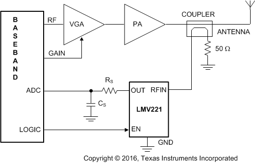 Figure 74. Transmit Power Control System
8.2.1.1 Design Requirements
Some of the design requirements for this logarithmic RMS power detector include:
Table 1. Design Parameters
| DESIGN PARAMETER | EXAMPLE VALUE |
|---|---|
| Supply voltage | 2.7 V |
| RF input frequency (unmodulated continuous wave) | 1855 MHz |
| Minimum input power for ELC = 1 dB | –42.9 dBm |
| Maximum input power for ELC = 1 dB | –5.5 dBm |
| Maximum output voltage, PIN = –5 dBm | 1.61 V |
8.2.1.2 Detailed Design Procedure
8.2.1.2.1 Detector Interfacing
For optimal performance of the LMV221 device, it is important that all its pins are connected to the surrounding circuitry in the appropriate way. Starting from the Functional Block Diagram the function of each pin is elaborated in the following sections. The details of the electrical interfacing are separately discussed for each pin. Output filtering options and the differences between single ended and differential interfacing with an ADC are also discussed in detail in the following subsections.
8.2.1.2.1.1 RF Input
RF parts typically use a characteristic impedance of 50 Ω. To comply with this standard the LMV221 has an input impedance of 50 Ω. Using a characteristic impedance other then 50 Ω causes a shift of the logarithmic intercept with respect to the value given in the 2.7-V DC and AC Electrical Characteristics. This intercept shift can be calculated according to Equation 13.

The intercept shifts to higher power levels for RSOURCE > 50 Ω, and shifts to lower power levels for RSOURCE < 50 Ω.
8.2.1.2.1.2 Output and Reference
The possible filtering techniques that can be applied to reduce ripple in the detector output voltage are discussed in Filtering. In addition, two different topologies to connect the LMV221 to an ADC are elaborated.
8.2.1.2.1.2.1 Filtering
The output voltage of the LMV221 is a measure for the applied RF signal on the RF input pin. Usually, the applied RF signal contains AM modulation that causes low frequency ripple in the detector output voltage. CDMA signals, for instance, contain a large amount of amplitude variations. Filtering of the output signal can be used to eliminate this ripple. The filtering can either be achieved by a low pass output filter or a low pass feedback filter. Those two techniques are shown in Figure 75 and Figure 76.
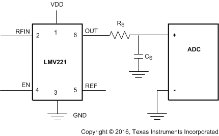 Figure 75. Low Pass Output Filter
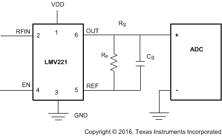 Figure 76. Low Pass Feedback Filter
Depending on the system requirements one of the these filtering techniques can be selected. The low pass output filter has the advantage that it preserves the output voltage when the LMV221 is brought into shutdown. This is elaborated in Output Behavior in Shutdown. In the feedback filter, resistor RP discharges capacitor CP in shutdown and therefore changes the output voltage of the device.
A disadvantage of the low pass output filter is that the series resistor RS limits the output drive capability. This may cause inaccuracies in the voltage read by an ADC when the ADC input impedance is not significantly larger than RS. In that case, the current flowing through the ADC input induces an error voltage across filter resistor RS. The low pass feedback filter does not have this disadvantage.
NOTE
Note that adding an external resistor between OUT and REF reduces the transfer gain (LOG-slope and LOG-intercept) of the device. The internal feedback resistor sets the gain of the transimpedance amplifier.
The filtering of the low pass output filter is achieved by resistor RS and capacitor CS. The −3 dB bandwidth of this filter can then be calculated by: ƒ−3 dB = 1 / 2πRSCS. The bandwidth of the low pass feedback filter is determined by external resistor RP in parallel with the internal resistor RTRANS, and external capacitor CP in parallel with internal capacitor CTRANS (see Figure 79). The −3 dB bandwidth of the feedback filter can be calculated by ƒ−3 dB = 1 / 2π (RP//RTRANS) (CP + CTRANS). The bandwidth set by the internal resistor and capacitor (when no external components are connected between OUT and REF) equals ƒ−3 dB = 1 / 2π RTRANS CTRANS = 450 kHz.
8.2.1.2.1.3 Interface to the ADC
The LMV221 can be connected to the ADC with a single-ended or a differential topology. The single ended topology connects the output of the LMV221 to the input of the ADC and the reference pin is not connected. In a differential topology, both the output and the reference pins of the LMV221 are connected to the ADC. The topologies are depicted in Figure 77 and Figure 78.
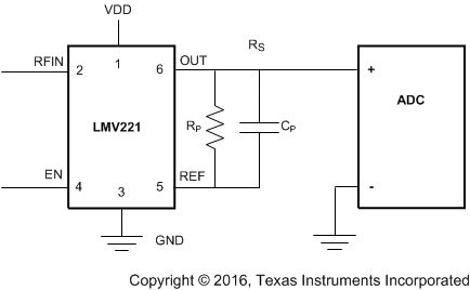 Figure 77. Single-Ended Application
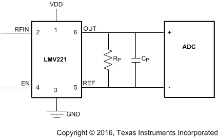 Figure 78. Differential Application
The differential topology has the advantage that it is compensated for temperature drift of the internal reference voltage. This can be explained by looking at the transimpedance amplifier of the LMV221 (Figure 79).
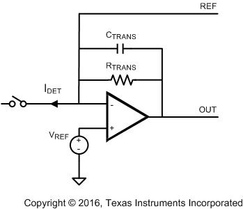 Figure 79. Output Stage of the LMV221
Equation 14 shows that the output of the amplifier is set by the detection current IDET multiplied by the resistor RTRANS plus the reference voltage VREF:
where
- IDET represents the detector current that is proportional to the RF input power.
Equation 14 shows that temperature variations in VREF are also present in the output VOUT. In case of a single ended topology the output is the only pin that is connected to the ADC. The ADC voltage for single ended is thus:
A differential topology also connects the reference pin, which is the value of reference voltage VREF. The ADC reads VOUT – VREF:
Equation 16 no longer contains the reference voltage VREF anymore. Temperature variations in this reference voltage are therefore not measured by the ADC.
8.2.1.3 Application Curves
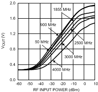
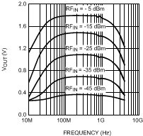
8.2.2 Application With Voltage Standing Wave Ratio (VSWR) Measurement
Transmission in RF systems requires matched termination by the proper characteristic impedance at the transmitter and receiver side of the link. In wireless transmission systems, however, matched termination of the antenna can rarely be achieved. The part of the transmitted power that is reflected at the antenna bounces back toward the PA and may cause standing waves in the transmission line between the PA and the antenna. These standing waves can attain unacceptable levels that may damage the PA. A VSWR measurement is used to detect such an occasion. It acts as an alarm function to prevent damage to the transmitter.
VSWR is defined as the ratio of the maximum voltage divided by the minimum voltage at a certain point on the transmission line:

where
- Γ = VREFLECTED / VFORWARD denotes the reflection coefficient.
This means that to determine the VSWR, both the forward (transmitted) and the reflected power levels must be measured. This can be accomplished by using two LMV221 RF power detectors according to Figure 82. A directional coupler is used to separate the forward and reflected power waves on the transmission line between the PA and the antenna. One secondary output of the coupler provides a signal proportional to the forward power wave, the other secondary output provides a signal proportional to the reflected power wave. The outputs of both RF detectors that measure these signals are connected to a microcontroller or baseband that calculates the VSWR from the detector output signals.
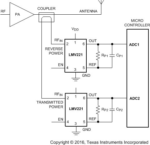 Figure 82. VSWR Application