SNOS018H August 1999 – December 2014 LMV331-N , LMV339-N , LMV393-N
PRODUCTION DATA.
- 1 Features
- 2 Applications
- 3 Description
- 4 Revision History
- 5 Pin Configuration and Functions
- 6 Specifications
- 7 Detailed Description
- 8 Application and Implementation
- 9 Power Supply Recommendations
- 10Layout
- 11Device and Documentation Support
- 12Mechanical, Packaging, and Orderable Information
Package Options
Mechanical Data (Package|Pins)
Thermal pad, mechanical data (Package|Pins)
Orderable Information
8 Application and Implementation
NOTE
Information in the following applications sections is not part of the TI component specification, and TI does not warrant its accuracy or completeness. TI’s customers are responsible for determining suitability of components for their purposes. Customers should validate and test their design implementation to confirm system functionality.
8.1 Application Information
8.1.1 Basic Comparator
The comparator compares the input voltage (VIN) at the non-inverting pin to the reference voltage (VREF) at the inverting pin. If VIN is less than VREF, the output voltage (VO) is at the saturation voltage. On the other hand, if VIN is greater than VREF, the output voltage (VO) is at VCC.
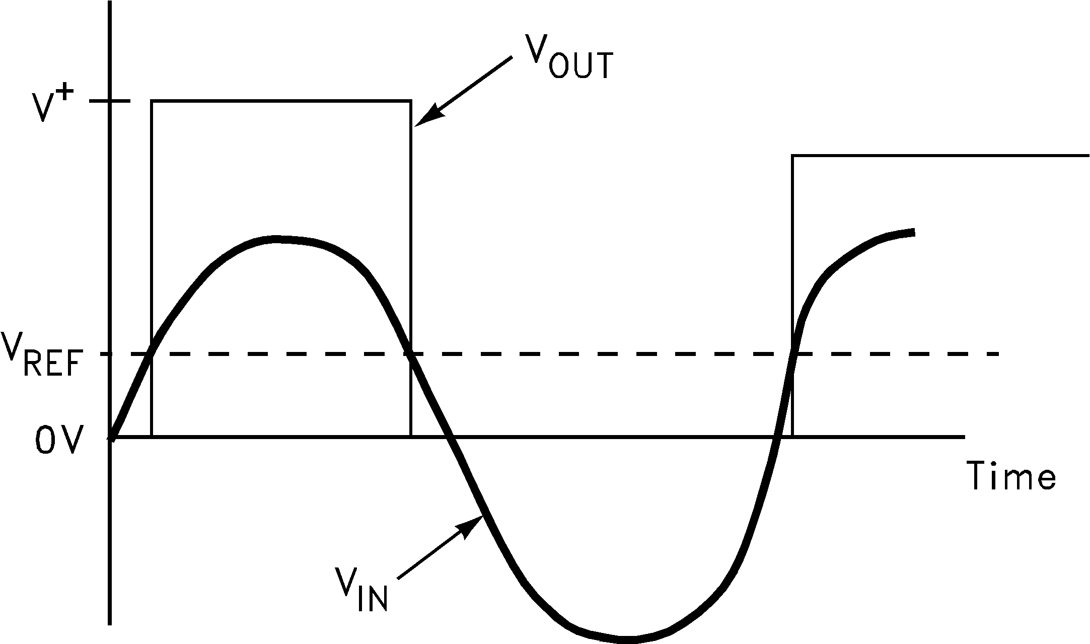
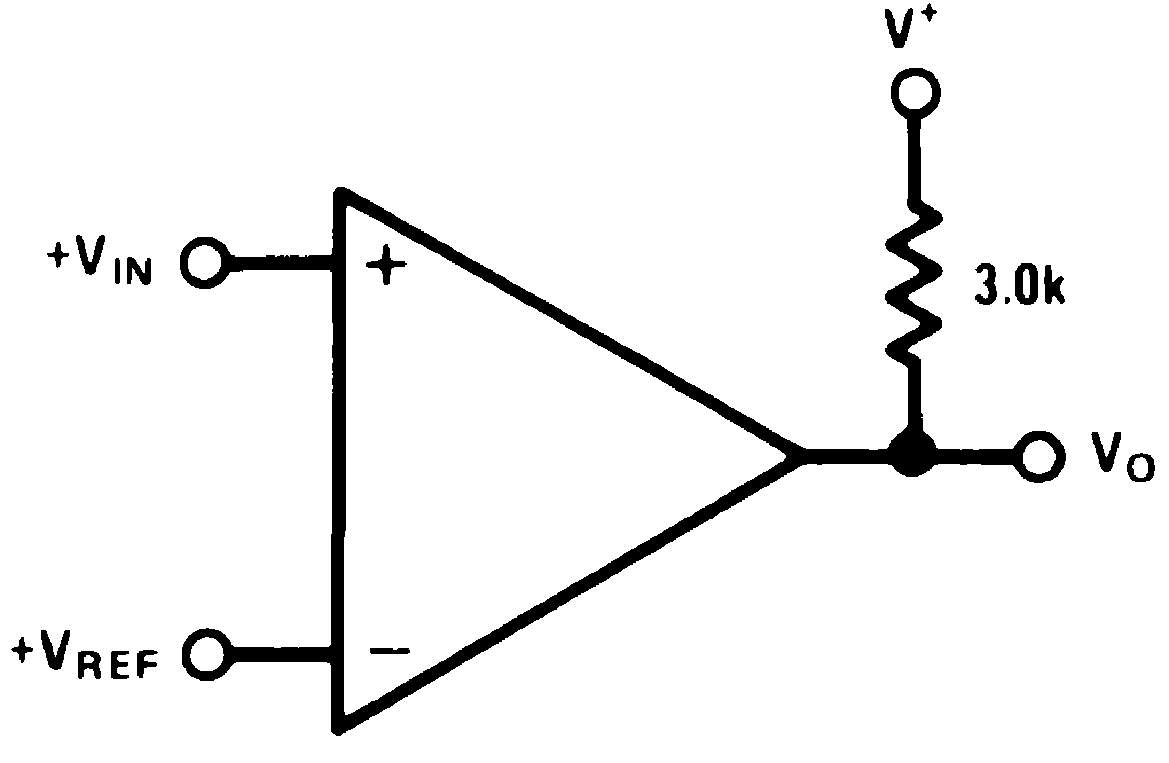 Figure 10. Basic Comparator
8.1.2 Comparator With Hysteresis
The basic comparator configuration may oscillate or produce a noisy output if the applied differential input voltage is near the comparator's offset voltage. This usually happens when the input signal is moving very slowly across the switching threshold of the comparator. This problem can be prevented by the addition of hysteresis or positive feedback.
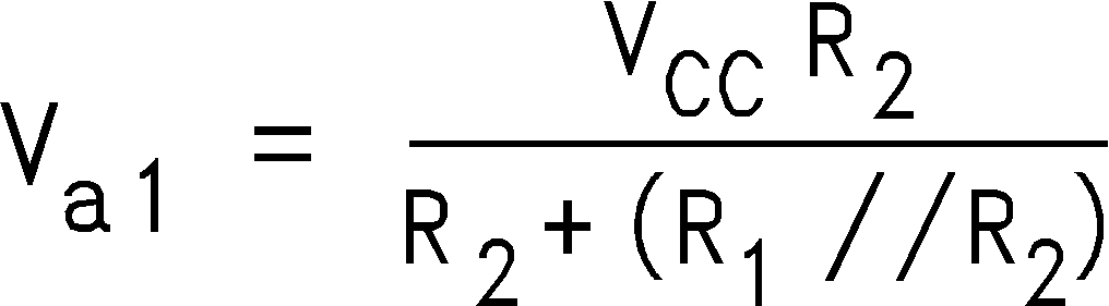
8.1.2.1 Inverting Comparator With Hysteresis
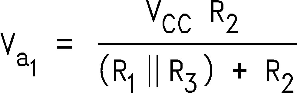
The inverting comparator with hysteresis requires a three resistor network that are referenced to the supply voltage VCC of the comparator. When Vin at the inverting input is less than Va, the voltage at the non-inverting node of the comparator (Vin < Va), the output voltage is high (for simplicity assume VO switches as high as VCC). The three network resistors can be represented as R1//R3 in series with R2. The lower input trip voltage Va1 is defined as:
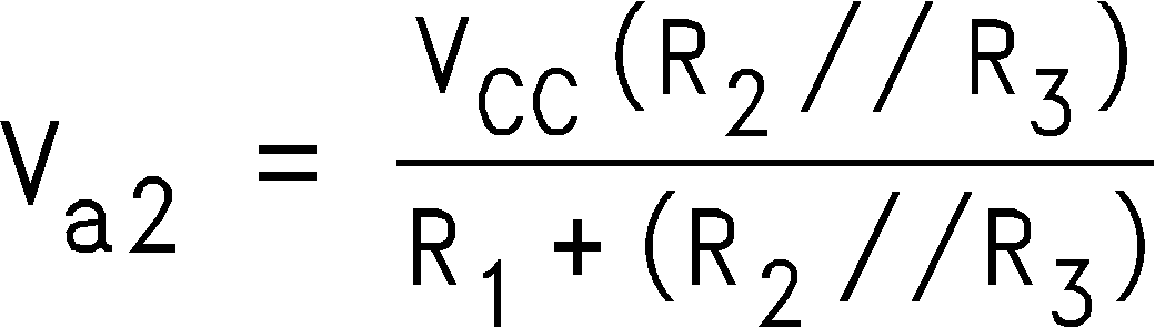
When Vin is greater than Va (Vin > Va), the output voltage is low very close to ground. In this case the three network resistors can be presented as R2//R3 in series with R1. The upper trip voltage Va2 is defined as:
The total hysteresis provided by the network is defined as:
To assure that the comparator will always switch fully to VCC and not be pulled down by the load the resistors values should be chosen as follow:
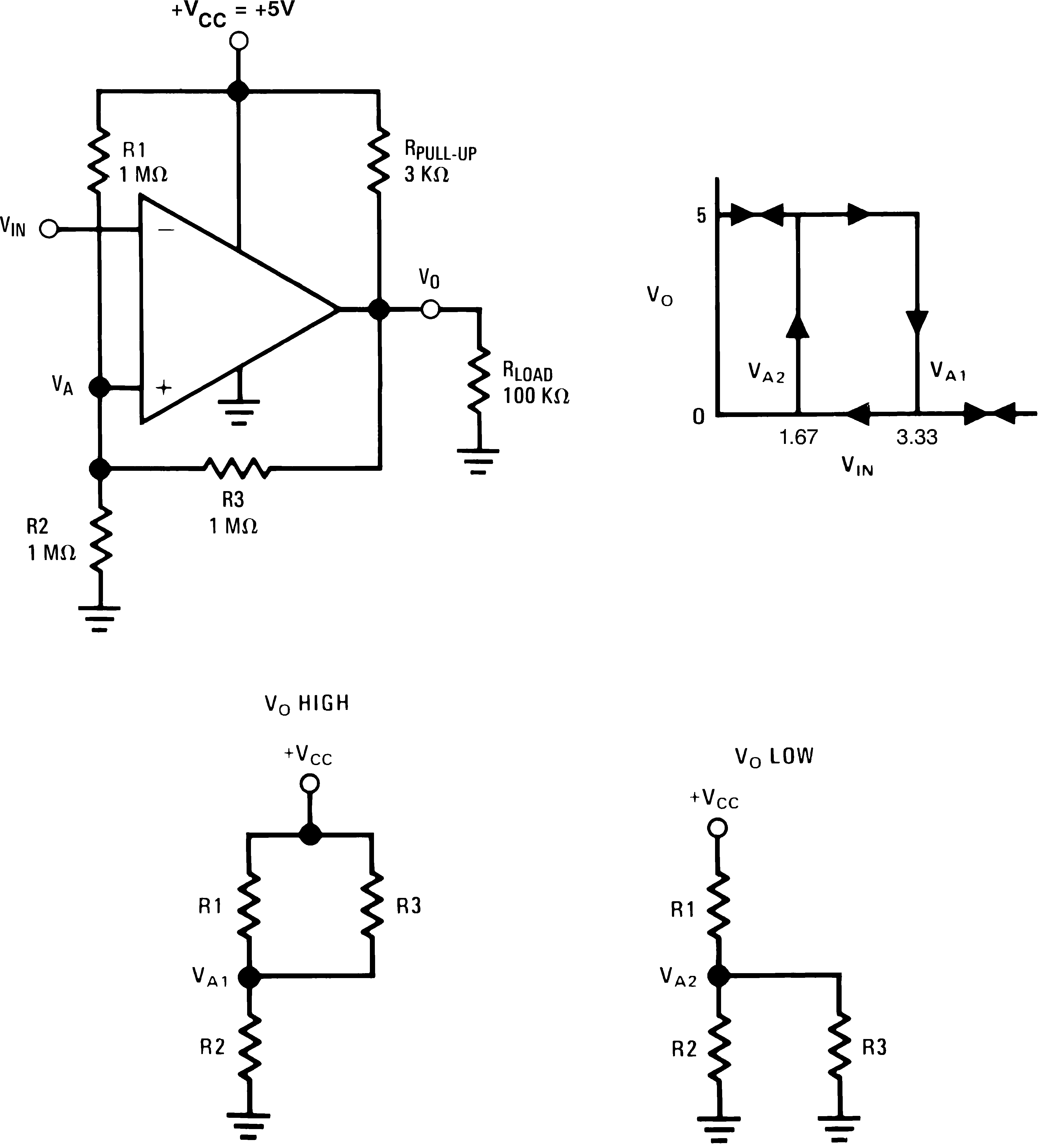 Figure 11. Inverting Comparator With Hysteresis
8.1.2.1.1 Non-inverting Comparator With Hysteresis
Non-inverting comparator with hysteresis requires a two resistor network, and a voltage reference (Vref) at the inverting input. When Vin is low, the output is also low. For the output to switch from low to high, Vin must rise up to Vin1 where Vin1 is calculated by:
When Vin is high, the output is also high. To make the comparator switch back to its low state, Vin must equal Vref before VA will again equal Vref. Vin can be calculated by:
The hysteresis of this circuit is the difference between Vin1 and Vin2.
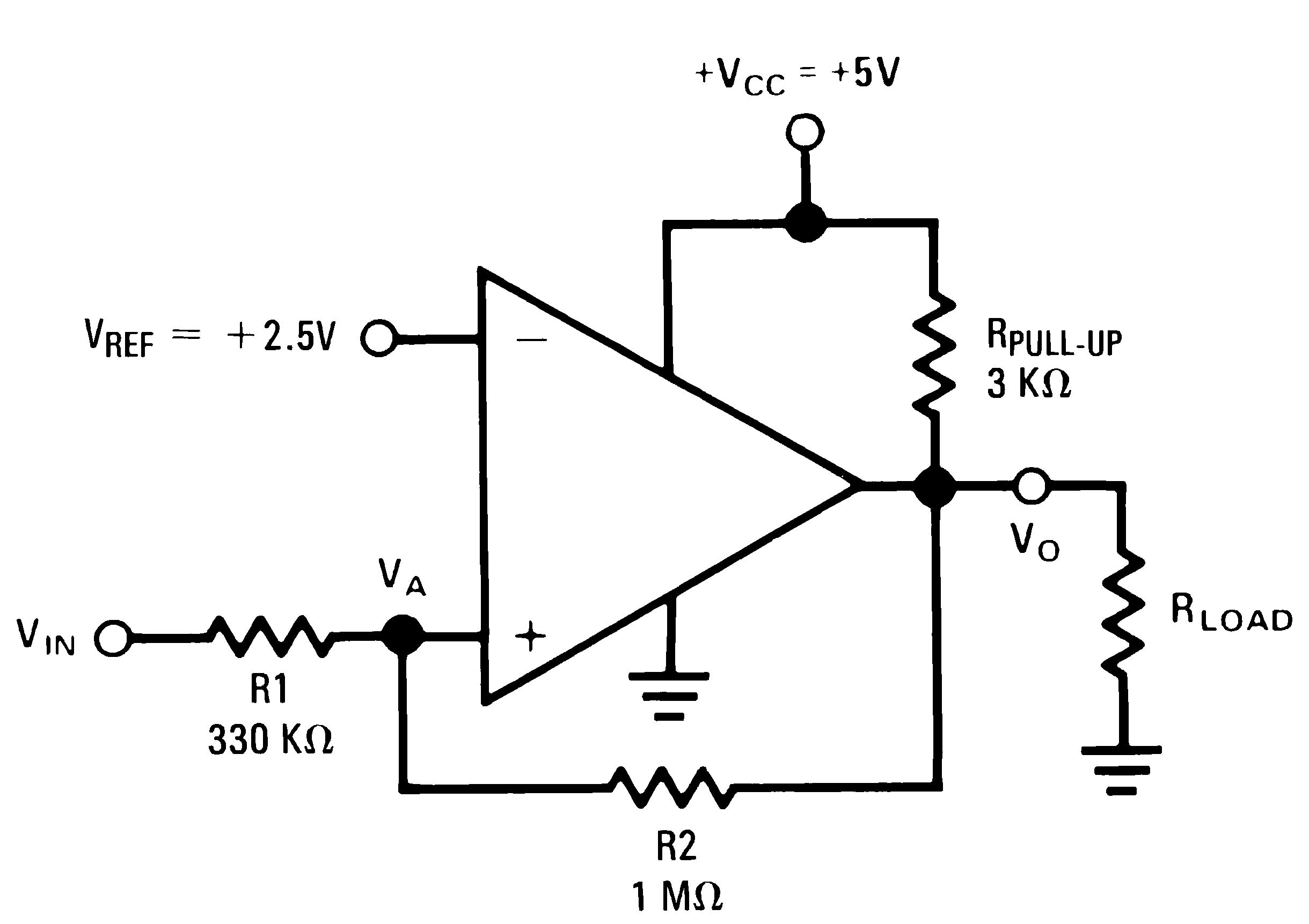 Figure 12. Noninverting Comparator With Hystersis
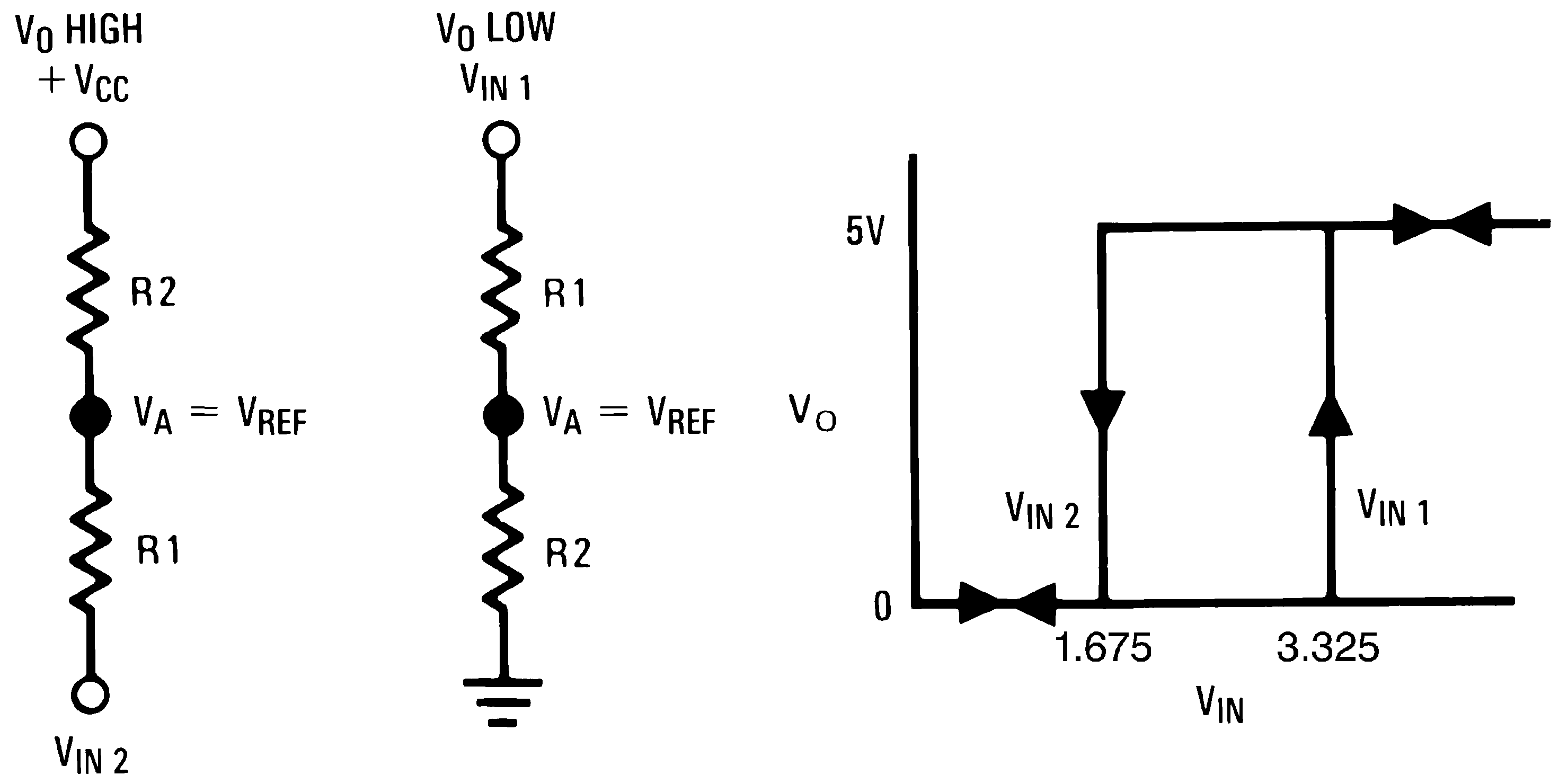 Figure 13. Hysteresis Threshold Points
8.1.3 ORing the Output
By the inherit nature of an open-collector comparator, the outputs of several comparators can be tied together with a shared pull-up resistor to VCC. If one or more of the comparators outputs goes low, the output VO will go low.
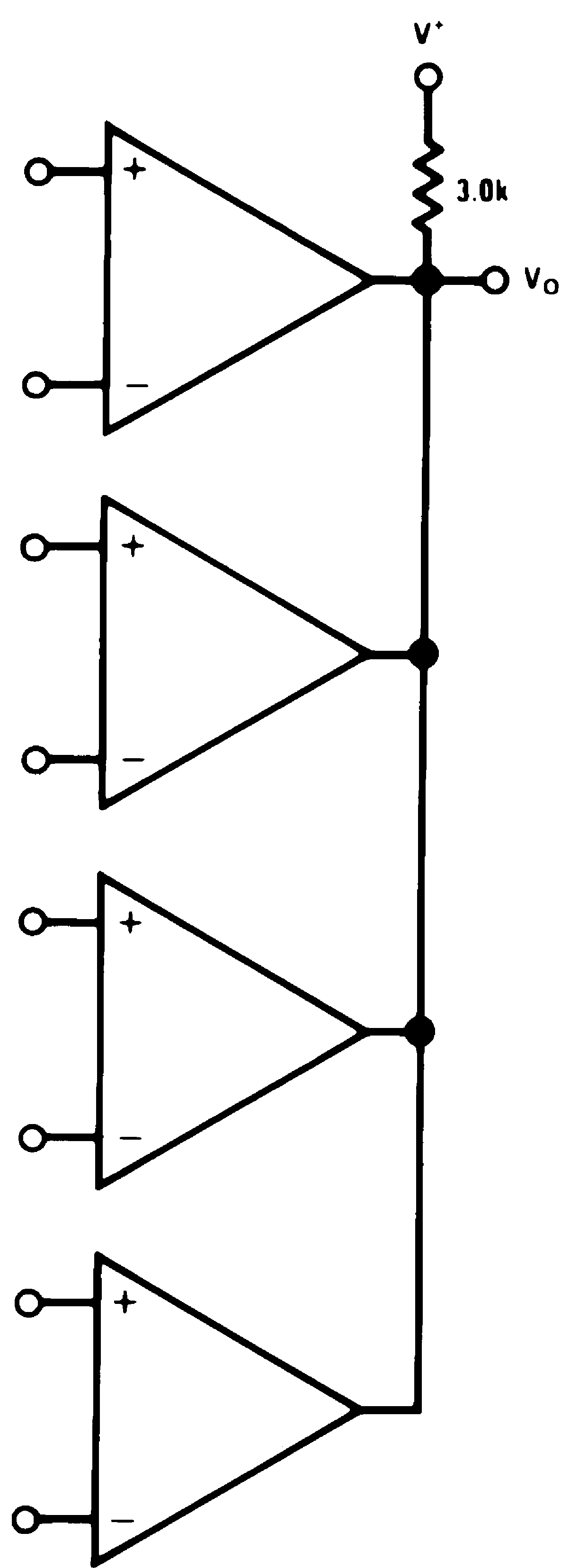 Figure 14. ORing the Outputs
8.1.4 Driving CMOS and TTL
The output of the comparator is capable of driving CMOS and TTL Logic circuits. The pull-up resistor may be pulled-up to any voltage equal to, or less than the supply voltage on V+. However, it must not be pulled-up to a voltage higher than V+.
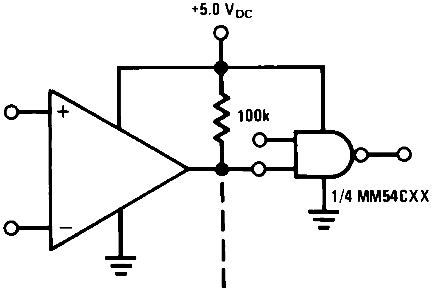 Figure 15. Driving CMOS
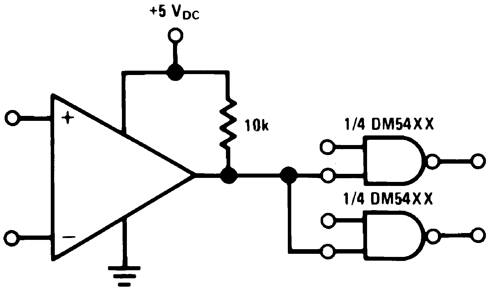 Figure 16. Driving TTL
8.1.5 AND Gates
The comparator can be used as three input AND gate. The operation of the gate is as follows:
The resistor divider at the inverting input establishes a reference voltage at that node. The non-inverting input is the sum of the voltages at the inputs divided by the voltage dividers. The output will go high only when all three inputs are high, casing the voltage at the non-inverting input to go above that at inverting input. The circuit values shown work for a 0 equal to ground and a 1 equal to 5 V.
The resistor values can be altered if different logic levels are desired. If more inputs are required, diodes are recommended to improve the voltage margin when all but one of the inputs are high.
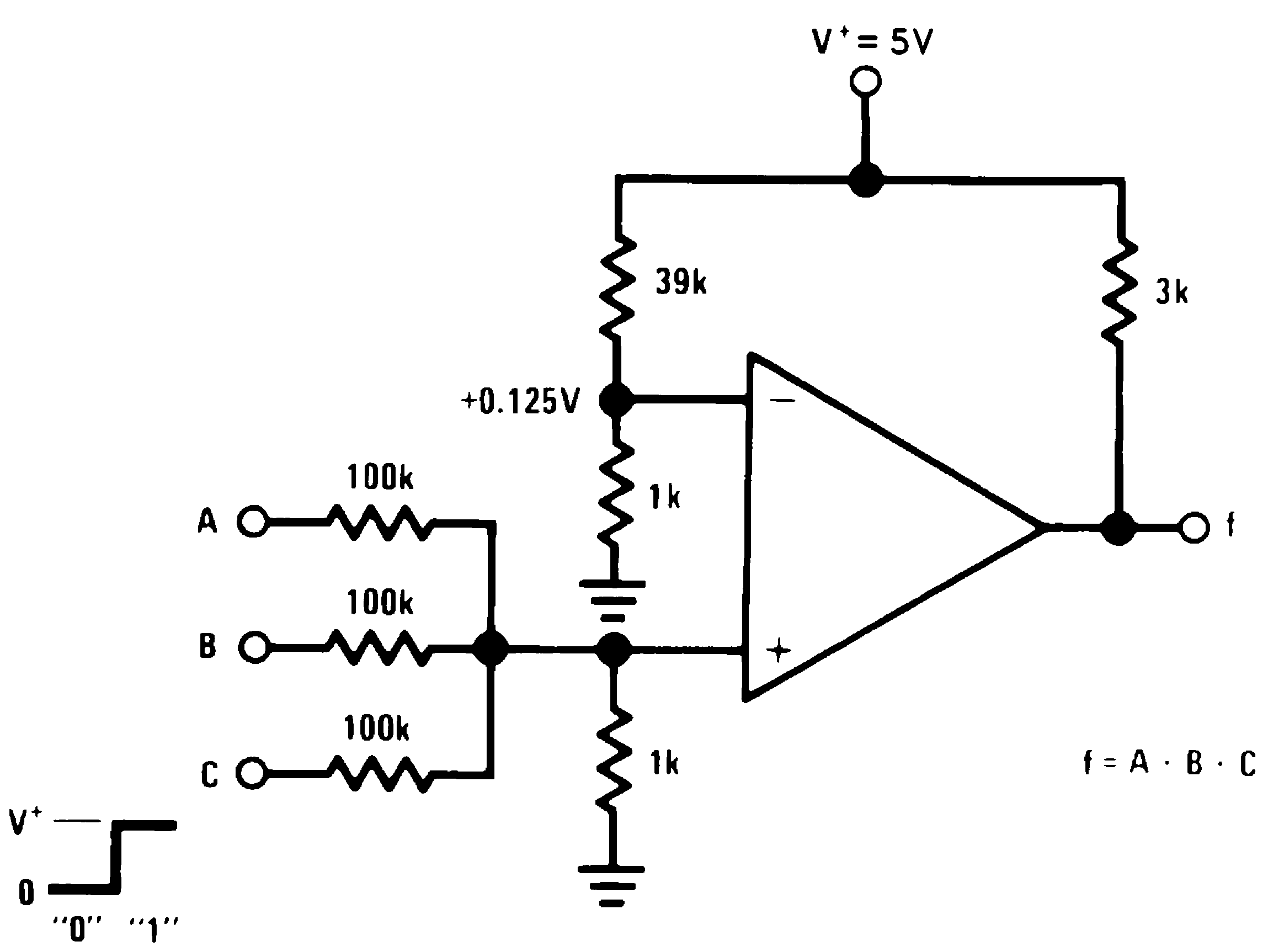 Figure 17. AND Gate
8.1.6 OR Gates
A three input OR gate is achieved from the basic AND gate simply by increasing the resistor value connected from the inverting input to Vcc, thereby reducing the reference voltage.
A logic 1 at any of the inputs will produce a logic 1 at the output.
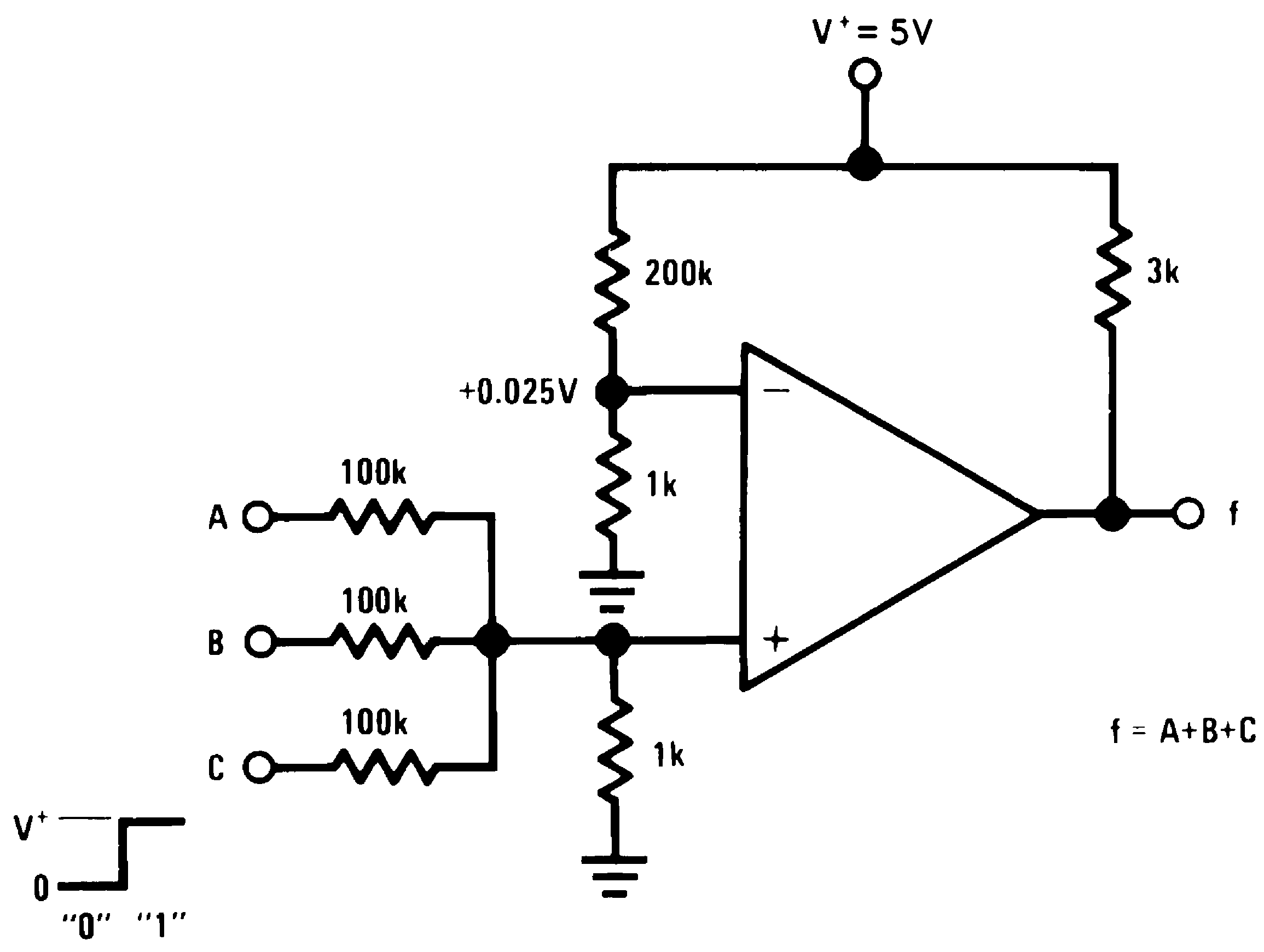 Figure 18. OR Gate
8.1.7 Large Fan-In Gate
Extra logic inputs may be added by ORing the input with multiple diodes.
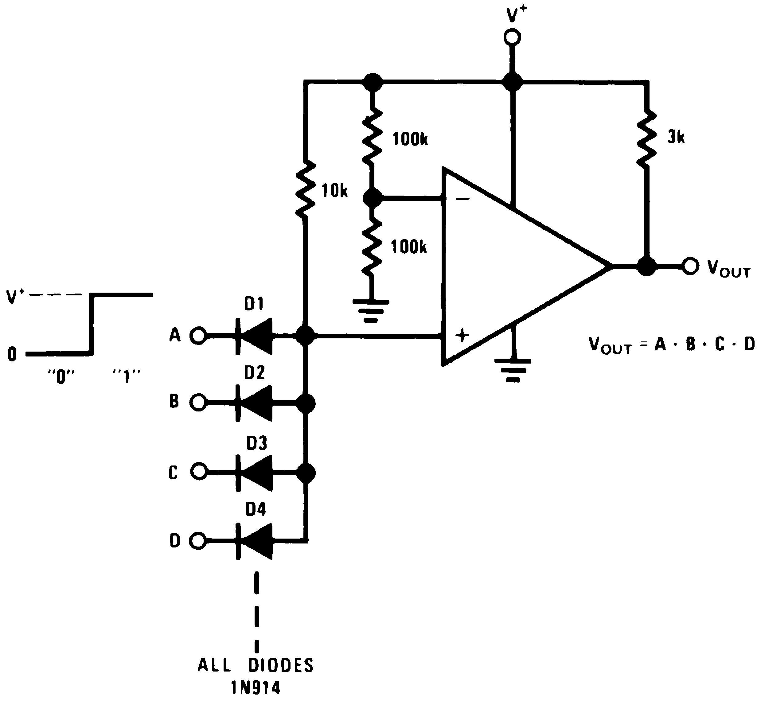 Figure 19. Large Fan-In and Gate
8.2 Typical Applications
8.2.1 Squarewave Oscillator
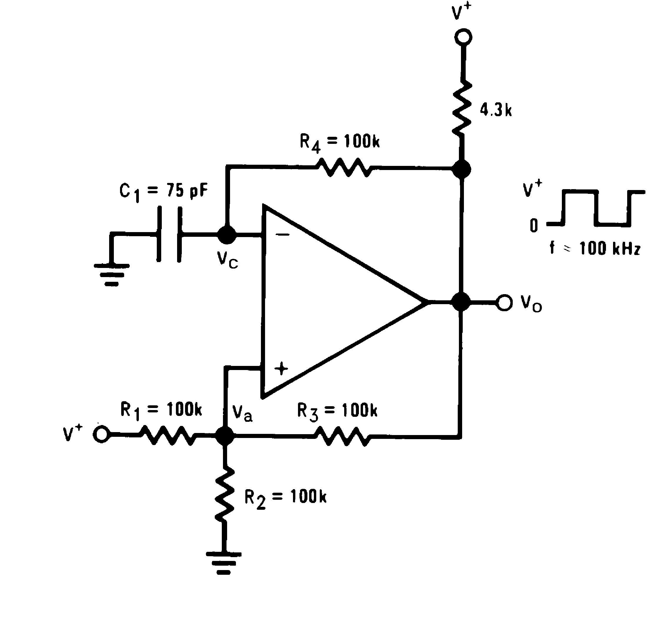 Figure 20. Squarewave Oscillator
8.2.1.1 Design Requirements
Comparators are ideal for oscillator applications. This square wave generator uses the minimum number of components. The output frequency is set by the RC time constant of the capacitor C1 and the resistor in the negative feedback R4. The maximum frequency is limited only by the large signal propagation delay of the comparator in addition to any capacitive loading at the output, which would degrade the output slew rate.
8.2.1.2 Detailed Design Procedure
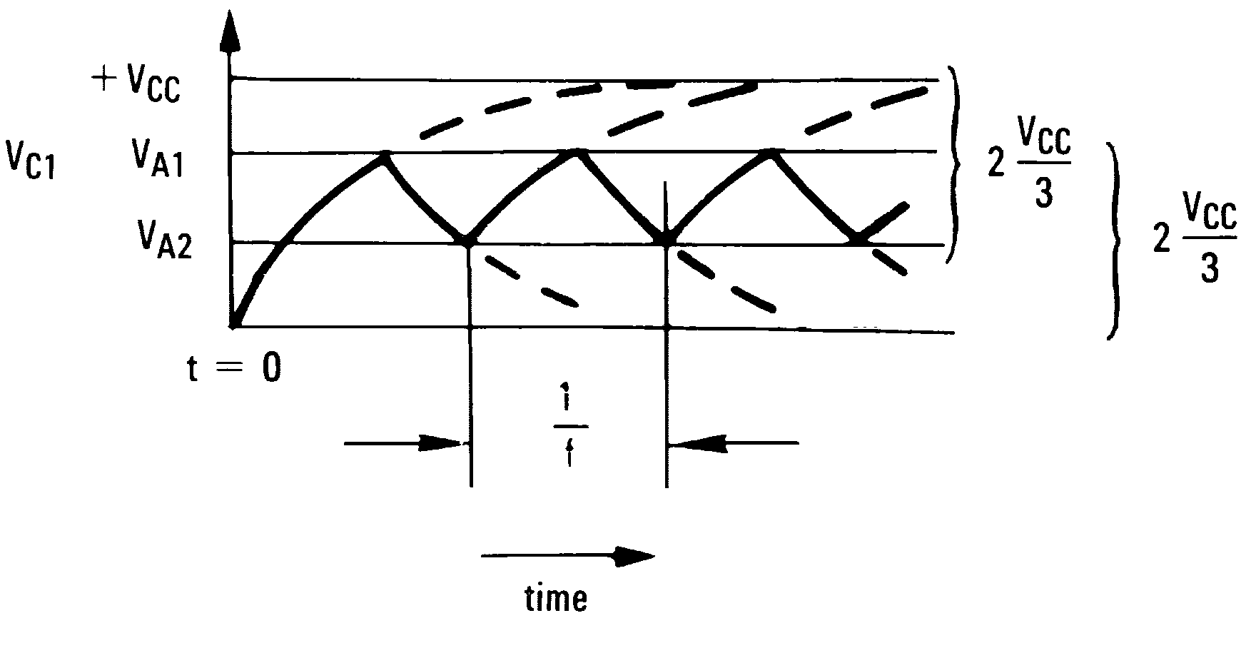 Figure 21. Squarewave Oscillator Timing Thresholds
To analyze the circuit, assume that the output is initially high. For this to be true, the voltage at the inverting input Vc has to be less than the voltage at the non-inverting input Va. For Vc to be low, the capacitor C1 has to be discharged and will charge up through the negative feedback resistor R4. When it has charged up to value equal to the voltage at the positive input Va1, the comparator output will switch.
Va1 will be given by:
If:
Then:
When the output switches to ground, the value of Va is reduced by the hysteresis network to a value given by:
Capacitor C1 must now discharge through R4 towards ground. The output will return to its high state when the voltage across the capacitor has discharged to a value equal to Va2.
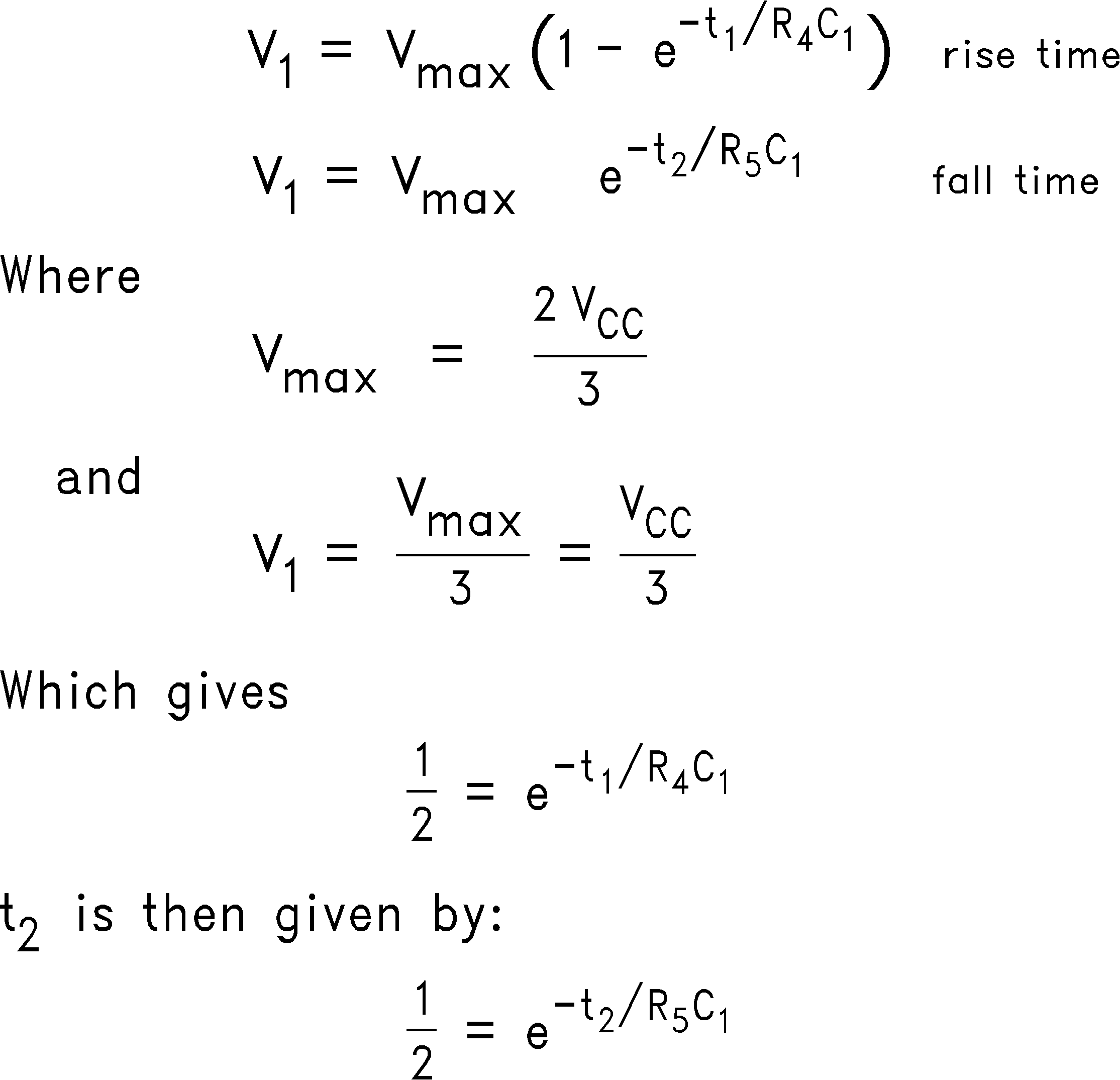
For the circuit shown, the period for one cycle of oscillation will be twice the time it takes for a single RC circuit to charge up to one half of its final value. The time to charge the capacitor can be calculated from:
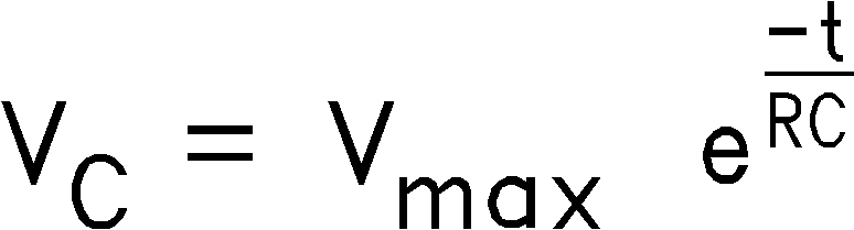
Where Vmax is the max applied potential across the capacitor = (2VCC/3)
and VC = Vmax/2 = VCC/3
One period will be given by:
or calculating the exponential gives:
Resistors R3 and R4 must be at least two times larger than R5 to ensure that VO will go all the way up to VCC in the high state. The frequency stability of this circuit should strictly be a function of the external components.
8.2.1.3 Application Curve
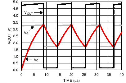 Figure 22. Waveforms for Circuit in Typical Applications
8.2.2 Crystal Controlled Oscillator
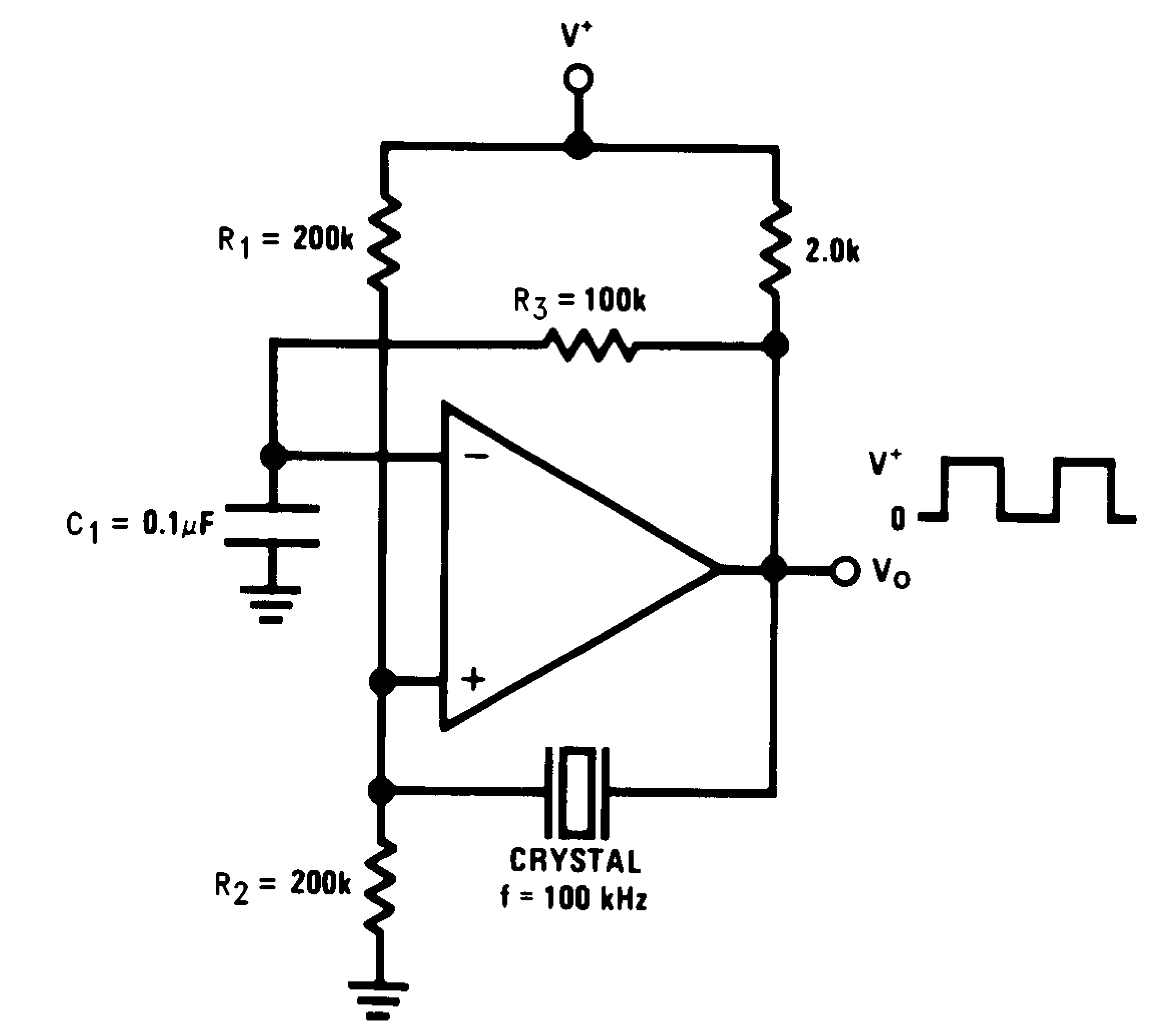 Figure 23. Crystal Controlled Oscillator
A simple yet very stable oscillator that generates a clock for slower digital systems can be obtained by using a resonator as the feedback element. It is similar to the squarewave oscillator, except that the positive feedback is obtained through a quartz crystal. The circuit oscillates when the transmission through the crystal is at a maximum, so the crystal in its series-resonant mode.
The value of R1 and R2 are equal so that the comparator will switch symmetrically about +VCC/2. The RC constant of R3 and C1 is set to be several times greater than the period of the oscillating frequency, insuring a 50% duty cycle by maintaining a DC voltage at the inverting input equal to the absolute average of the output waveform.
When specifying the crystal, be sure to order series resonant with the desired temperature coefficient.
8.2.3 Pulse Generator With Variable Duty Cycle
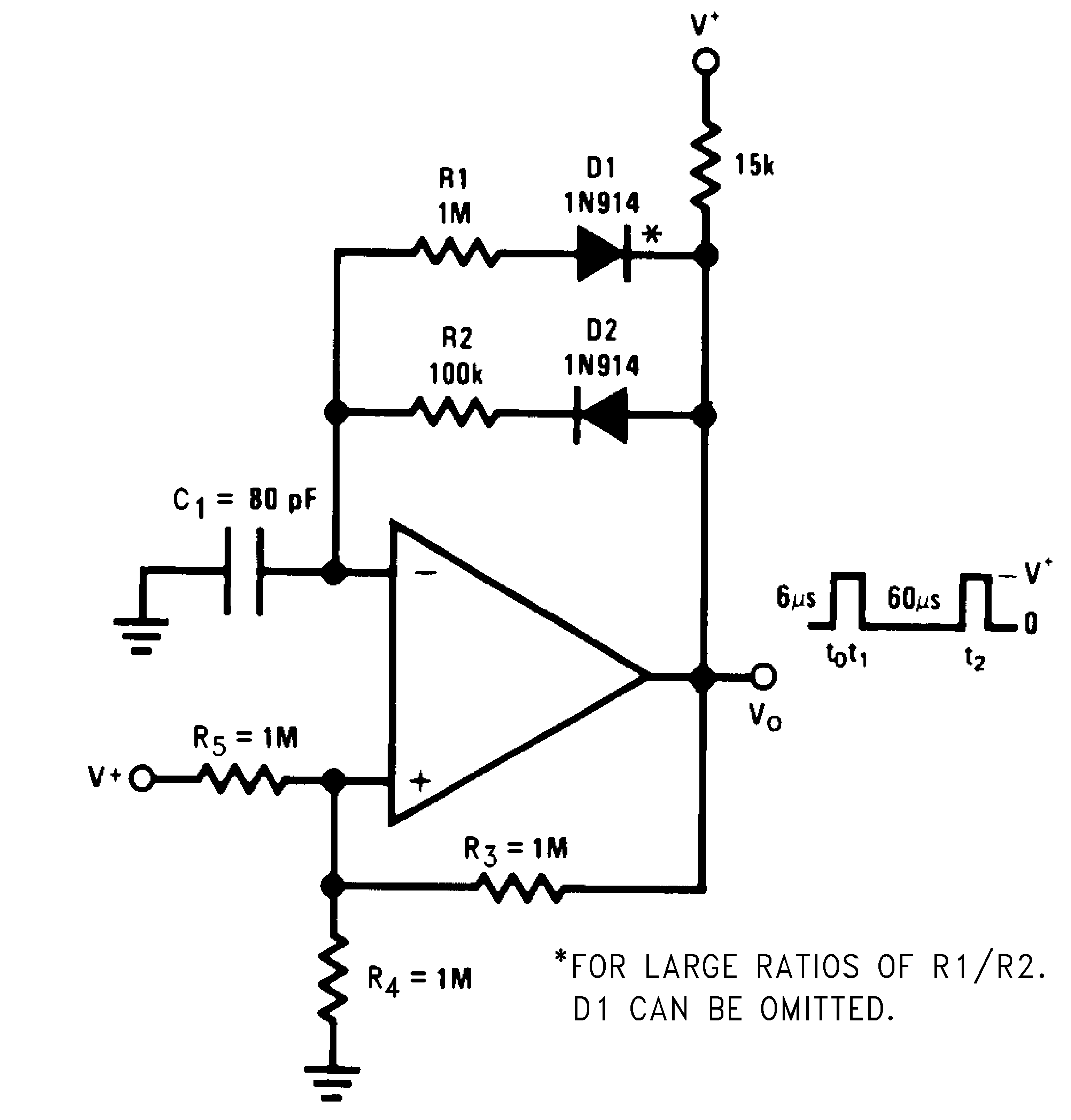 Figure 24. Pulse Generator With Variable Duty Cycle
The pulse generator with variable duty cycle is just a minor modification of the basic square wave generator. Providing a separate charge and discharge path for capacitor C1generates a variable duty cycle. One path, through R2 and D2 will charge the capacitor and set the pulse width (t1). The other path, R1 and D1 will discharge the capacitor and set the time between pulses (t2).
By varying resistor R1, the time between pulses of the generator can be changed without changing the pulse width. Similarly, by varying R2, the pulse width will be altered without affecting the time between pulses. Both controls will change the frequency of the generator. The pulse width and time between pulses can be found from:
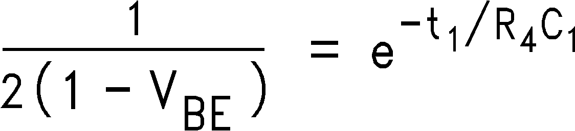
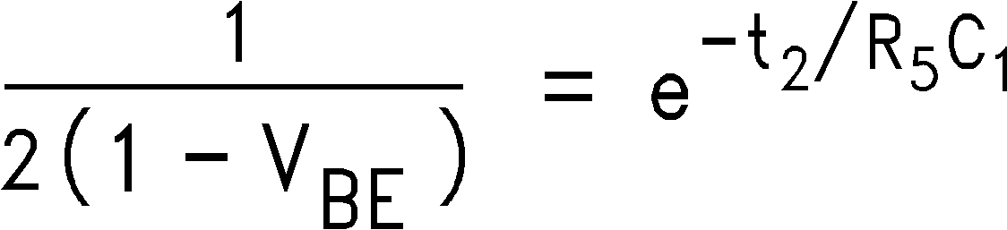
Solving these equations for t1 and t2
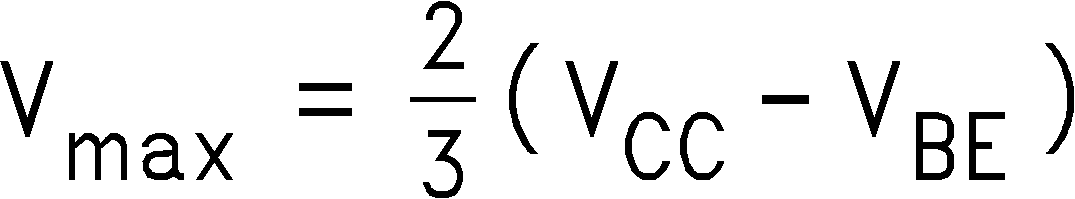
These terms will have a slight error due to the fact that Vmax is not exactly equal to 2/3 VCC but is actually reduced by the diode drop to:
8.2.4 Positive Peak Detector
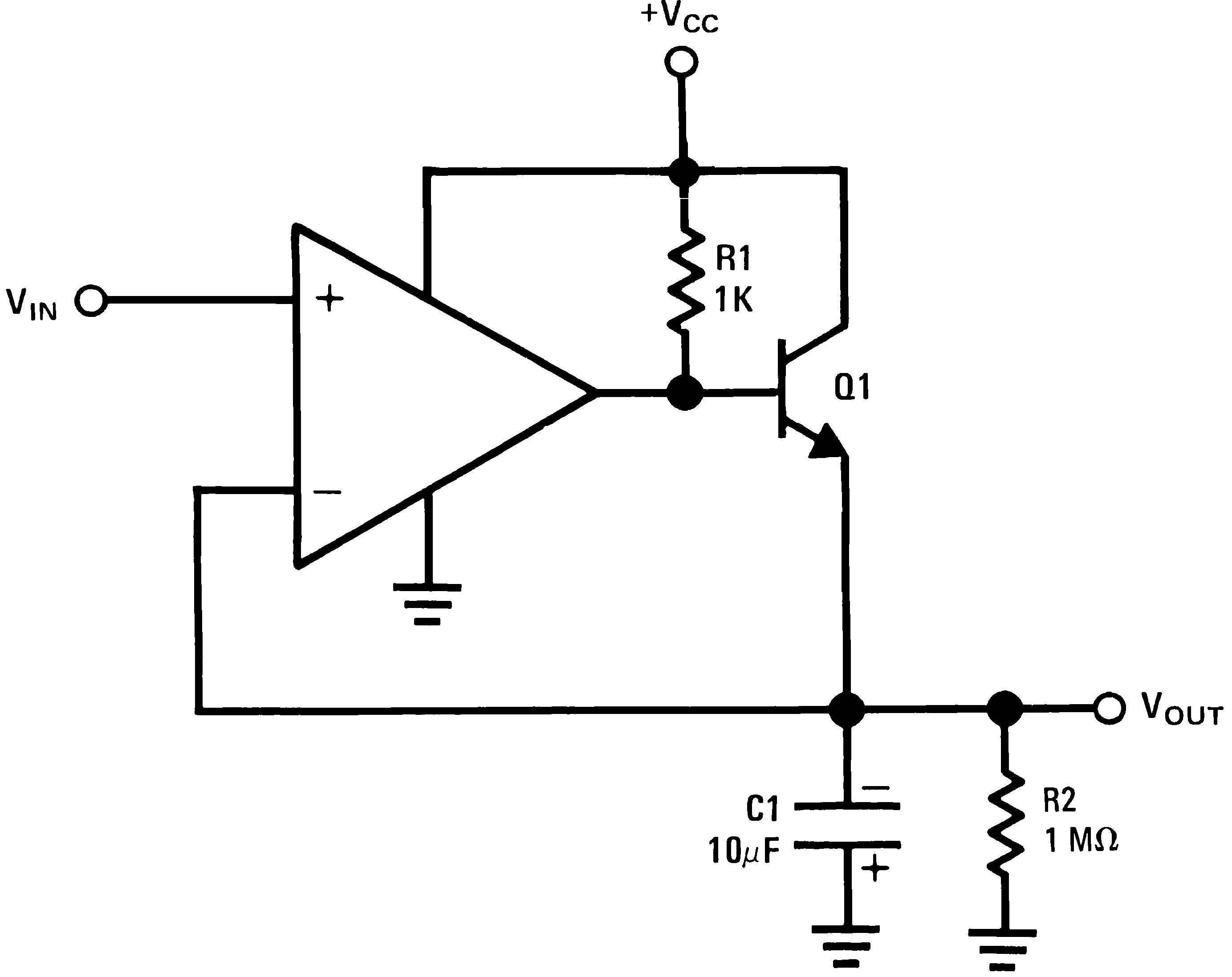 Figure 25. Positive Peak Detector
Positive peak detector is basically the comparator operated as a unit gain follower with a large holding capacitor from the output to ground. Additional transistor is added to the output to provide a low impedance current source. When the output of the comparator goes high, current is passed through the transistor to charge up the capacitor. The only discharge path will be the 1-MΩ resistor shunting C1 and any load that is connected to the output. The decay time can be altered simply by changing the 1-MΩ resistor. The output should be used through a high impedance follower to a avoid loading the output of the peak detector.
8.2.5 Negative Peak Detector
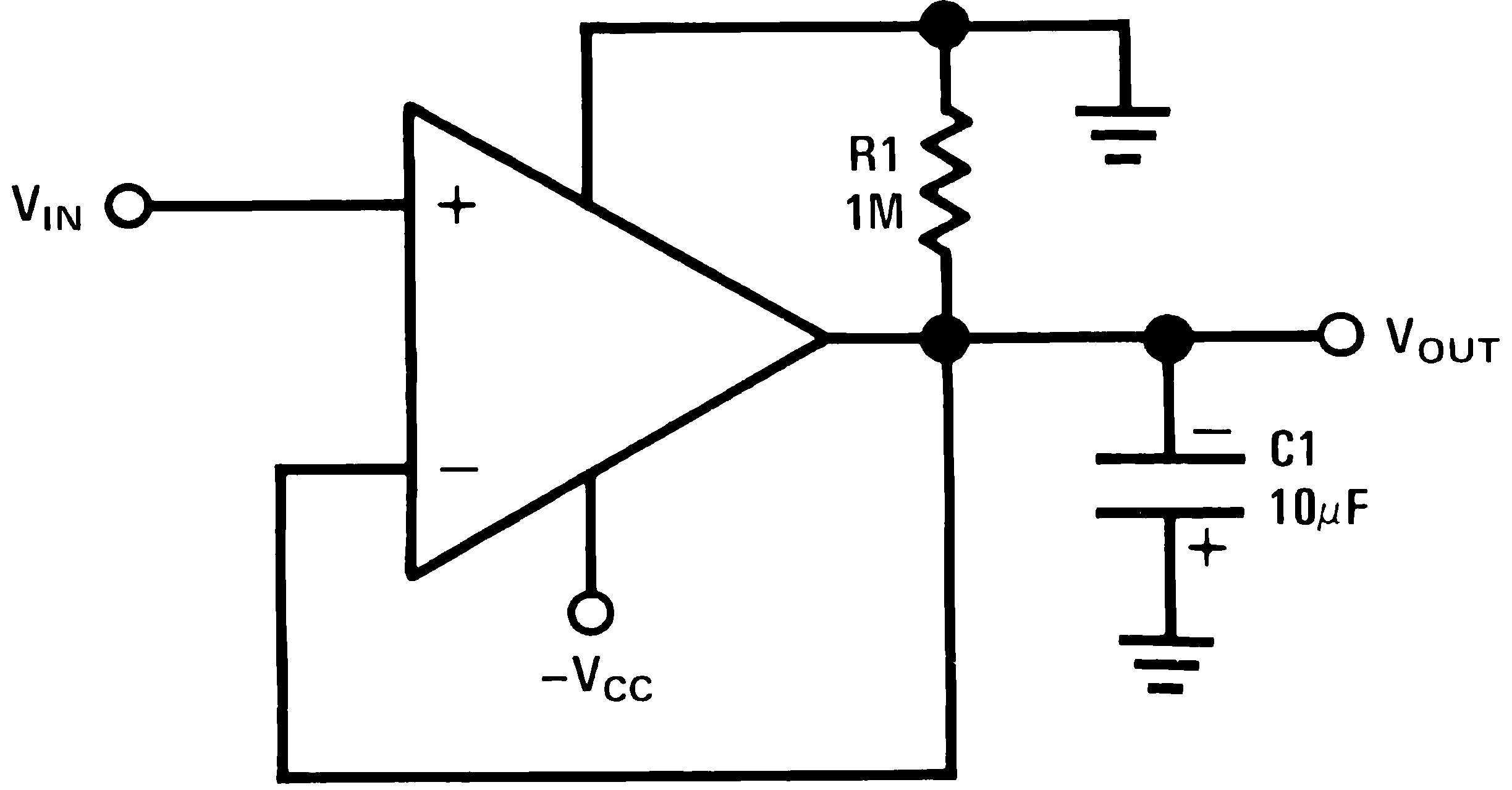 Figure 26. Negative Peak Detector
For the negative detector, the output transistor of the comparator acts as a low impedance current sink. The only discharge path will be the 1-MΩ resistor and any load impedance used. Decay time is changed by varying the 1-MΩ resistor.