SNOS018H August 1999 – December 2014 LMV331-N , LMV339-N , LMV393-N
PRODUCTION DATA.
- 1 Features
- 2 Applications
- 3 Description
- 4 Revision History
- 5 Pin Configuration and Functions
- 6 Specifications
- 7 Detailed Description
- 8 Application and Implementation
- 9 Power Supply Recommendations
- 10Layout
- 11Device and Documentation Support
- 12Mechanical, Packaging, and Orderable Information
Package Options
Mechanical Data (Package|Pins)
Thermal pad, mechanical data (Package|Pins)
Orderable Information
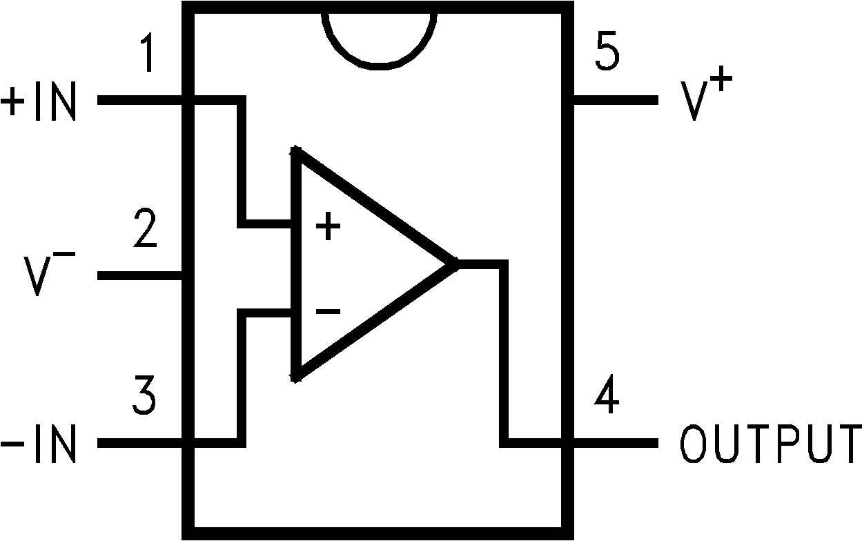
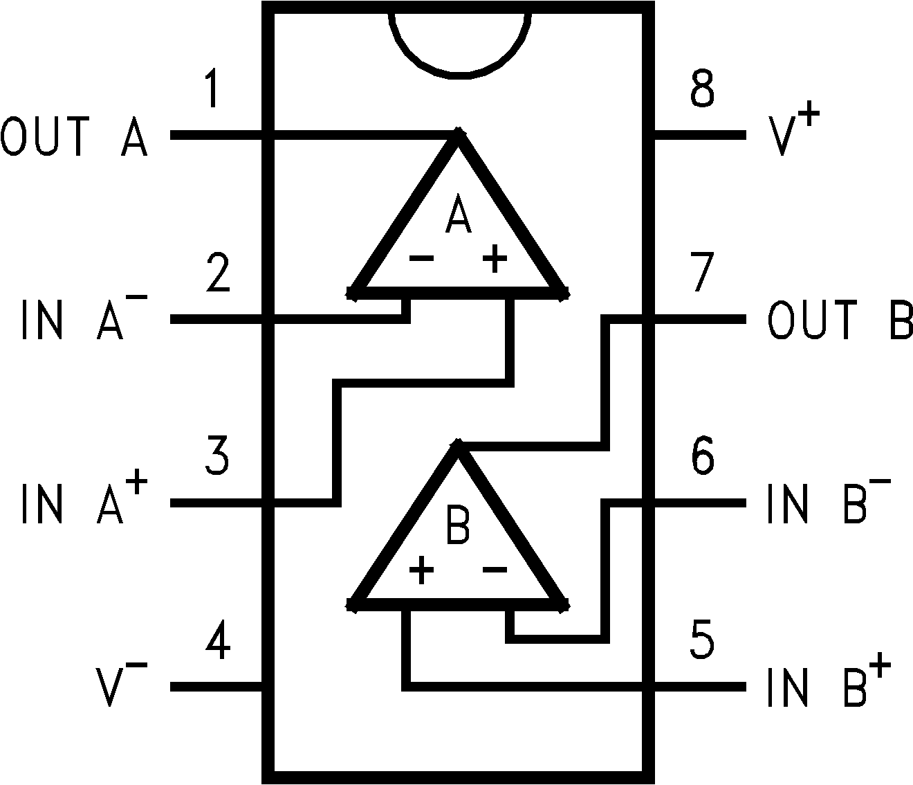
5 Pin Configuration and Functions
DCK and DBV Package
5-Pin SC70 / SOT23
Top View
D and DGK Package
8-Pin SOIC / VSSOP
Top View
D and PW Package
14-Pin SOIC / TSSOP
Top View
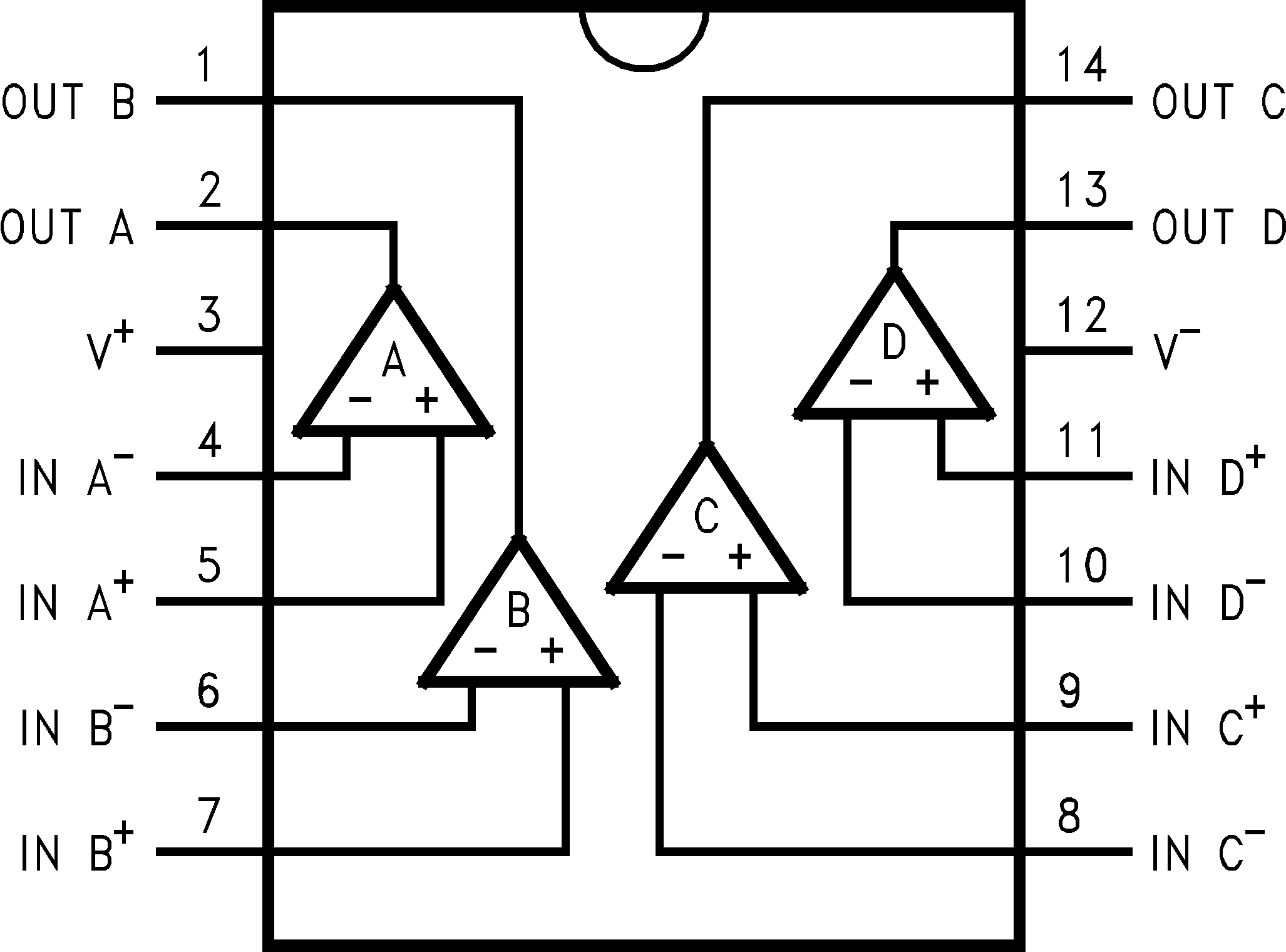
Pin Functions
| PIN | TYPE | DESCRIPTION | |||
|---|---|---|---|---|---|
| NAME | LMV331-N DVB,DCK |
LMV393-N D,DGK |
LMV339-N PW |
||
| +IN | 1 | - | - | I | Noninverting input |
| +IN A | - | 3 | 5 | I | Noninverting input, channel A |
| +IN B | - | 5 | 7 | I | Noninverting input, channel B |
| +IN C | - | - | 9 | I | Noninverting input, channel C |
| +IN D | - | - | 11 | I | Noninverting input, channel D |
| -IN | 3 | - | - | I | Inverting input |
| -IN A | - | 2 | 4 | I | Inverting input, channel A |
| -IN B | - | 6 | 6 | I | Inverting input, channel B |
| -IN C | - | - | 8 | I | Inverting input, channel C |
| -IN D | - | - | 10 | I | Inverting input, channel D |
| OUT | 4 | - | - | O | Output |
| OUT A | - | 1 | 2 | O | Output, channel A |
| OUT B | - | 7 | 1 | O | Output, channel B |
| OUT C | - | - | 14 | O | Output, channel C |
| OUT D | - | - | 13 | O | Output, channel D |
| V+ | 5 | 8 | 3 | P | Positive (highest) power supply |
| V- | 2 | 4 | 12 | P | Negative (lowest) power supply |