SNOS018H August 1999 – December 2014 LMV331-N , LMV339-N , LMV393-N
PRODUCTION DATA.
- 1 Features
- 2 Applications
- 3 Description
- 4 Revision History
- 5 Pin Configuration and Functions
- 6 Specifications
- 7 Detailed Description
- 8 Application and Implementation
- 9 Power Supply Recommendations
- 10Layout
- 11Device and Documentation Support
- 12Mechanical, Packaging, and Orderable Information
Package Options
Mechanical Data (Package|Pins)
Thermal pad, mechanical data (Package|Pins)
Orderable Information
6 Specifications
6.1 Absolute Maximum Ratings
over operating free-air temperature range (unless otherwise noted)(1)(3)| MIN | MAX | UNIT | ||
|---|---|---|---|---|
| Differential Input Voltage | ±Supply Voltage | |||
| Voltage on any pin (referred to V− pin) | 5.5 | V | ||
| Soldering Information | ||||
| Infrared or Convection (20 sec) | 235 | °C | ||
| Junction Temperature (2) | 150 | °C | ||
| Storage temperature, Tstg | −65 | 150 | °C | |
(1) Stresses beyond those listed under Absolute Maximum Ratings may cause permanent damage to the device. These are stress ratings only, which do not imply functional operation of the device at these or any other conditions beyond those indicated under Recommended Operating Conditions. Exposure to absolute-maximum-rated conditions for extended periods may affect device reliability.
(2) The maximum power dissipation is a function of TJ(MAX), θJA. The maximum allowable power dissipation at any ambient temperature is PD = (TJ(MAX) - TA)/θJA. All numbers apply for packages soldered directly onto a PC board.
(3) If Military/Aerospace specified devices are required, please contact the Texas Instruments Sales Office / Distributors for availability and specifications.
6.2 ESD Ratings
| VALUE | UNIT | |||
|---|---|---|---|---|
| V(ESD) | Electrostatic discharge | Human-body model (HBM), per ANSI/ESDA/JEDEC JS-001(1) | ±800 | V |
| Machine model | ±120 | |||
(1) JEDEC document JEP155 states that 500-V HBM allows safe manufacturing with a standard ESD control process.
6.3 Recommended Operating Conditions
over operating free-air temperature range (unless otherwise noted)(1)| MIN | MAX | UNIT | ||
|---|---|---|---|---|
| Supply Voltage | 2.7 | 5 | V | |
| Temperature Range (2) | −40 | 85 | °C | |
(1) Stresses beyond those listed under Absolute Maximum Ratings may cause permanent damage to the device. These are stress ratings only, which do not imply functional operation of the device at these or any other conditions beyond those indicated under Recommended Operating Conditions. Exposure to absolute-maximum-rated conditions for extended periods may affect device reliability.
(2) The maximum power dissipation is a function of TJ(MAX), θJA. The maximum allowable power dissipation at any ambient temperature is PD = (TJ(MAX) - TA)/θJA. All numbers apply for packages soldered directly onto a PC board.
6.4 Thermal Information
| THERMAL METRIC(1) | LMV331-N | LMV339-N | LMV393-N | UNIT | ||||
|---|---|---|---|---|---|---|---|---|
| DCK | DBV | D | PW | D | DGK | |||
| 5 PINS | 5 PINS | 14 PINS | 14 PINS | 8 PINS | 8 PINS | |||
| RθJA | Junction-to-ambient thermal resistance | 478 | 265 | 145 | 155 | 190 | 23 | °C/W |
(1) For more information about traditional and new thermal metrics, see the IC Package Thermal Metrics application report, SPRA953.
6.5 2.7-V DC Electrical Characteristics
Unless otherwise specified, all limits ensured for TJ = 25°C, V+ = 2.7V, V− = 0V.| PARAMETER | TEST CONDITIONS | MIN (1) |
TYP (2) |
MAX (1) |
UNIT | |
|---|---|---|---|---|---|---|
| VOS | Input Offset Voltage | 1.7 | 7 | mV | ||
| TCVOS | Input Offset Voltage Average Drift | At the temperature extremes | 5 | µV/°C | ||
| IB | Input Bias Current | 10 | 250 | nA | ||
| At the temperature extremes | 400 | |||||
| IOS | Input Offset Current | 5 | 50 | nA | ||
| At the temperature extremes | 150 | |||||
| VCM | Input Voltage Range | −0.1 | V | |||
| 2.0 | V | |||||
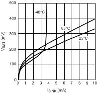
| VSAT | Saturation Voltage | ISINK ≤ 1 mA | 120 | mV | ||
| IO | Output Sink Current | VO ≤ 1.5V | 5 | 23 | mA | |
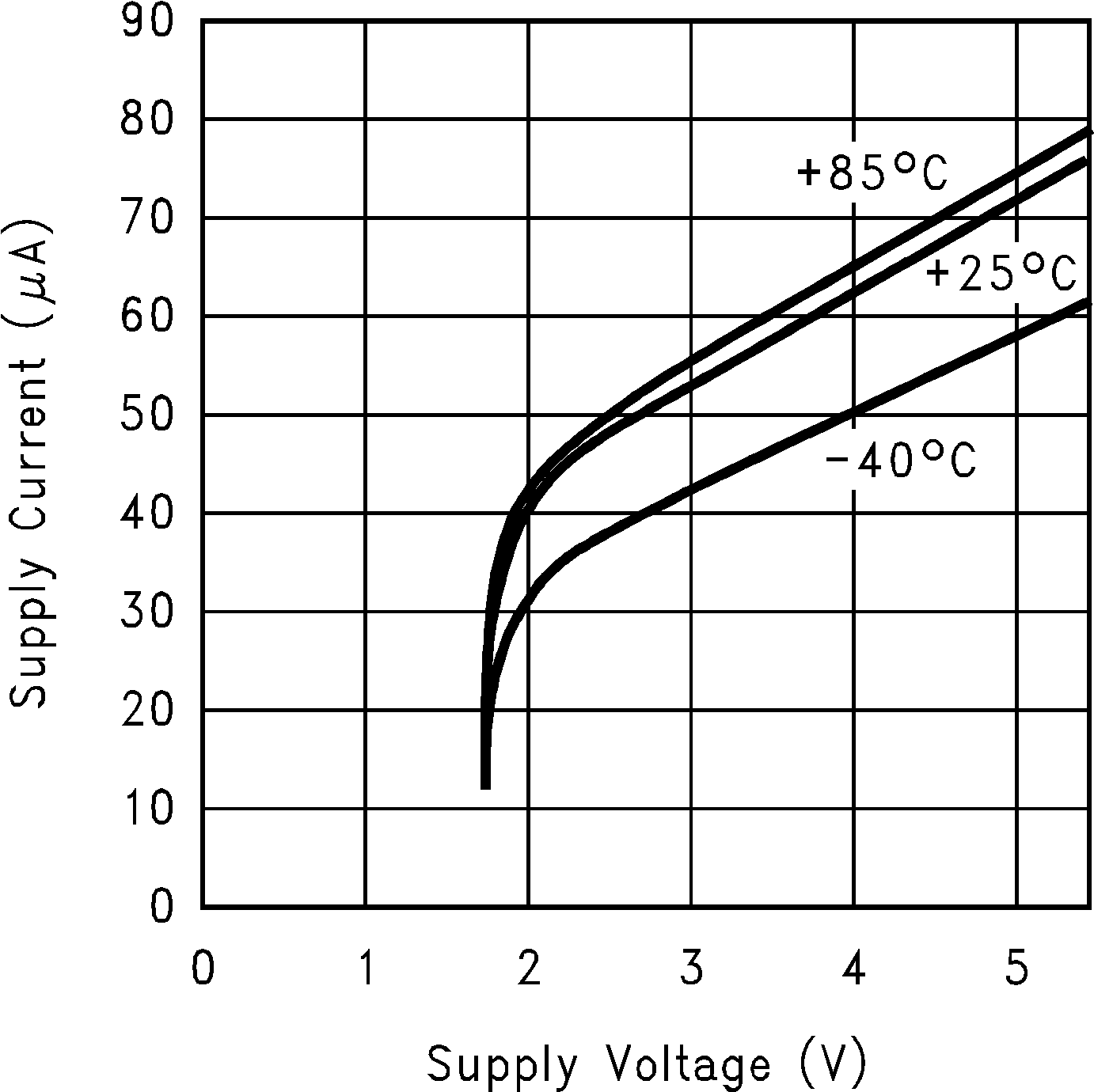
| IS | Supply Current | LMV331-N | 40 | 100 | µA | |
| LMV393-N Both Comparators |
70 | 140 | µA | |||
| LMV339-N All four Comparators |
140 | 200 | µA | |||
| Output Leakage Current | .003 | µA | ||||
| At the temperature extremes | 1 |
(1) All limits are ensured by testing or statistical analysis.
(2) Typical values represent the most likely parametric norm as determined at the time of characterization. Actual typical values may vary over time and will also depend on the application and configuration. The typical values are not tested and are not ensured on shipped production material.
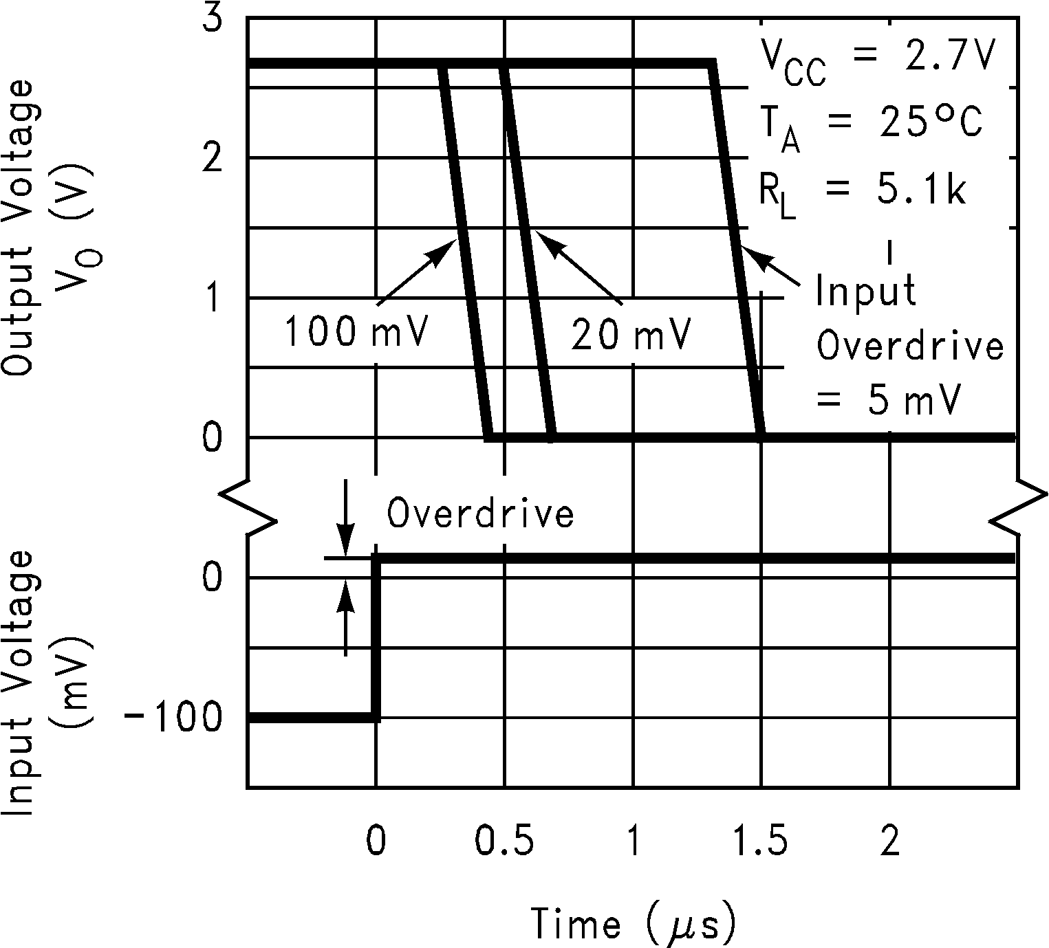
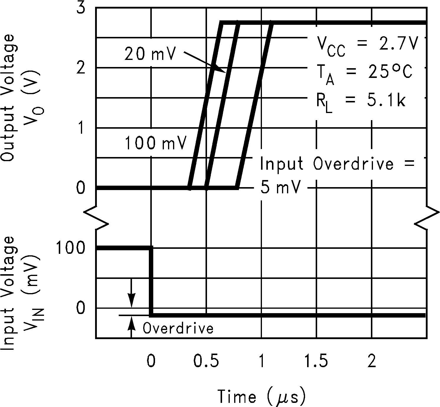
6.6 2.7-V AC Electrical Characteristics
TJ = 25°C, V+ = 2.7 V, RL = 5.1 kΩ, V− = 0 V.| PARAMETER | TEST CONDITIONS | MIN (1) |
TYP (2) |
MAX (1) |
UNIT | |
|---|---|---|---|---|---|---|
| tPHL | Propagation Delay (High to Low) | Input Overdrive = 10 mV | 1000 | ns | ||
| Input Overdrive = 100 mV | 350 | ns | ||||
| tPLH | Propagation Delay (Low to High) | Input Overdrive = 10 mV | 500 | ns | ||
| Input Overdrive = 100 mV | 400 | ns |
(1) All limits are ensured by testing or statistical analysis.
(2) Typical values represent the most likely parametric norm as determined at the time of characterization. Actual typical values may vary over time and will also depend on the application and configuration. The typical values are not tested and are not ensured on shipped production material.
6.7 5-V DC Electrical Characteristics
Unless otherwise specified, all limits ensured for TJ = 25°C, V+ = 5 V, V− = 0 V.| PARAMETER | TEST CONDITIONS | MIN (1) |
TYP (2) |
MAX (1) |
UNIT | |
|---|---|---|---|---|---|---|
| VOS | Input Offset Voltage | 1.7 | 7 | mV | ||
| At the temperature extremes | 9 | |||||
| TCVOS | Input Offset Voltage Average Drift | 5 | µV/°C | |||
| IB | Input Bias Current | 25 | 250 | nA | ||
| At the temperature extremes | 400 | |||||
| IOS | Input Offset Current | 2 | 50 | nA | ||
| At the temperature extremes | 150 | |||||
| VCM | Input Voltage Range | −0.1 | V | |||
| 4.2 | V | |||||
| AV | Voltage Gain | 20 | 50 | V/mV | ||
| Vsat | Saturation Voltage | ISINK ≤ 4 mA | 200 | 400 | mV | |
| At the temperature extremes | 700 | |||||
| IO | Output Sink Current | VO ≤ 1.5V | 84 | 10 | mA | |
| IS | Supply Current | LMV331-N | 60 | 120 | µA | |
| At the temperature extremes | 150 | |||||
| LMV393-N Both Comparators |
100 | 200 | µA | |||
| At the temperature extremes | 250 | |||||
| LMV339-N All four Comparators |
170 | 300 |
µA | |||
| At the temperature extremes | 350 | |||||
| Output Leakage Current | .003 | µA | ||||
| At the temperature extremes | 1 |
(1) All limits are ensured by testing or statistical analysis.
(2) Typical values represent the most likely parametric norm as determined at the time of characterization. Actual typical values may vary over time and will also depend on the application and configuration. The typical values are not tested and are not ensured on shipped production material.
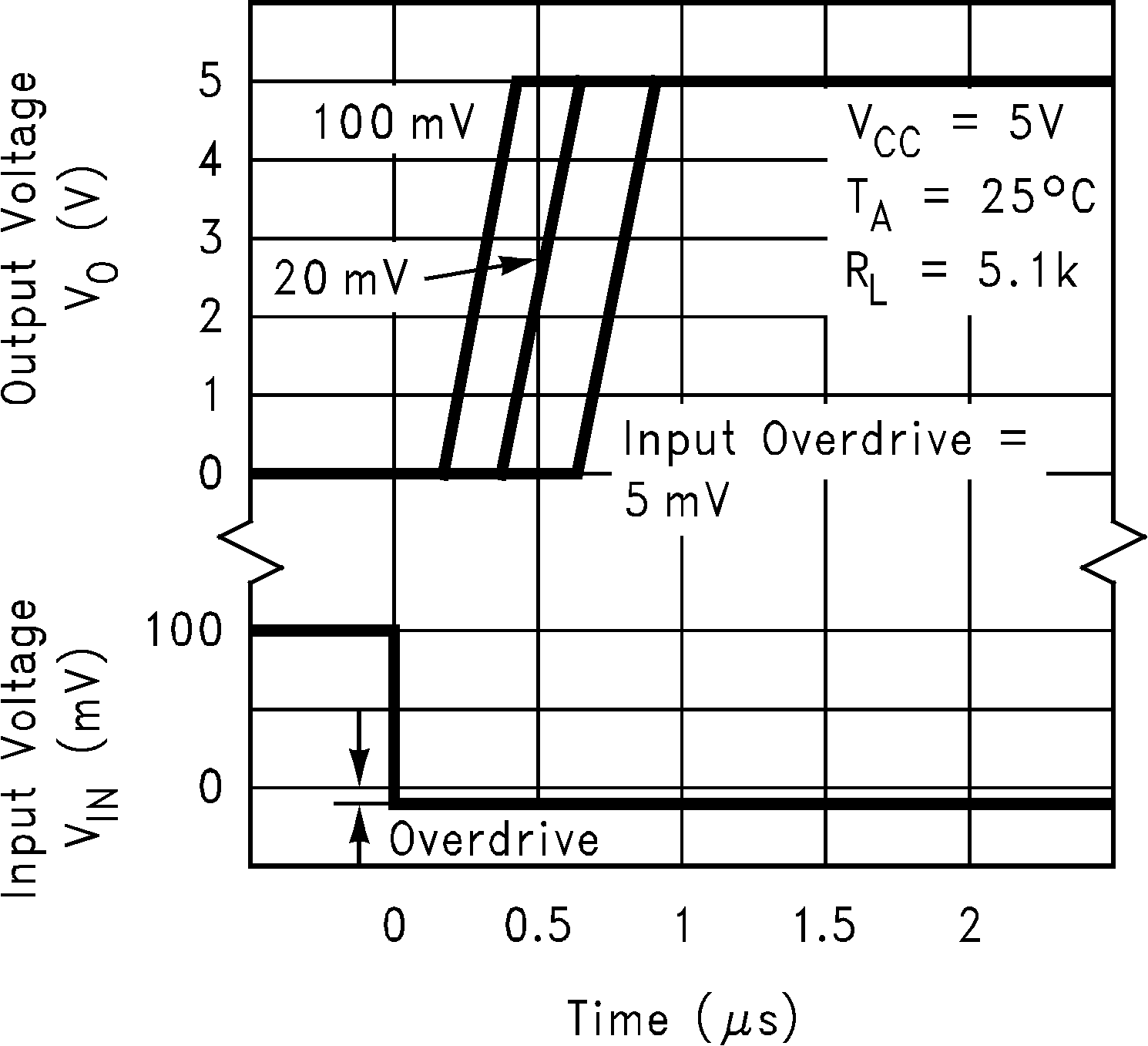
6.8 5-V AC Electrical Characteristics
TJ = 25°C, V+ = 5 V, RL = 5.1 kΩ, V− = 0 V.| PARAMETER | TEST CONDITIONS | MIN (1) |
TYP (2) |
MAX (1) |
UNIT | |
|---|---|---|---|---|---|---|
| tPHL | Propagation Delay (High to Low) | Input Overdrive = 10 mV | 600 | ns | ||
| Input Overdrive = 100 mV | 200 | ns | ||||
| tPLH | Propagation Delay (Low to High) | Input Overdrive = 10 mV | 450 | ns | ||
| Input Overdrive = 100 mV | 300 | ns |
(1) All limits are ensured by testing or statistical analysis.
(2) Typical values represent the most likely parametric norm as determined at the time of characterization. Actual typical values may vary over time and will also depend on the application and configuration. The typical values are not tested and are not ensured on shipped production material.
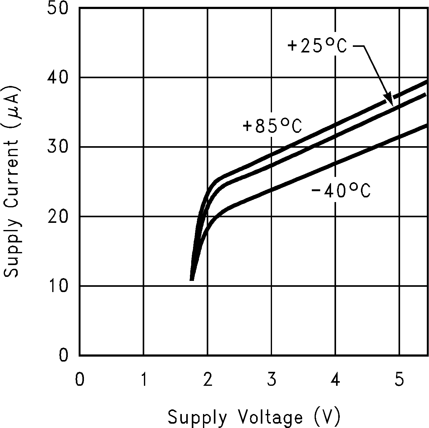
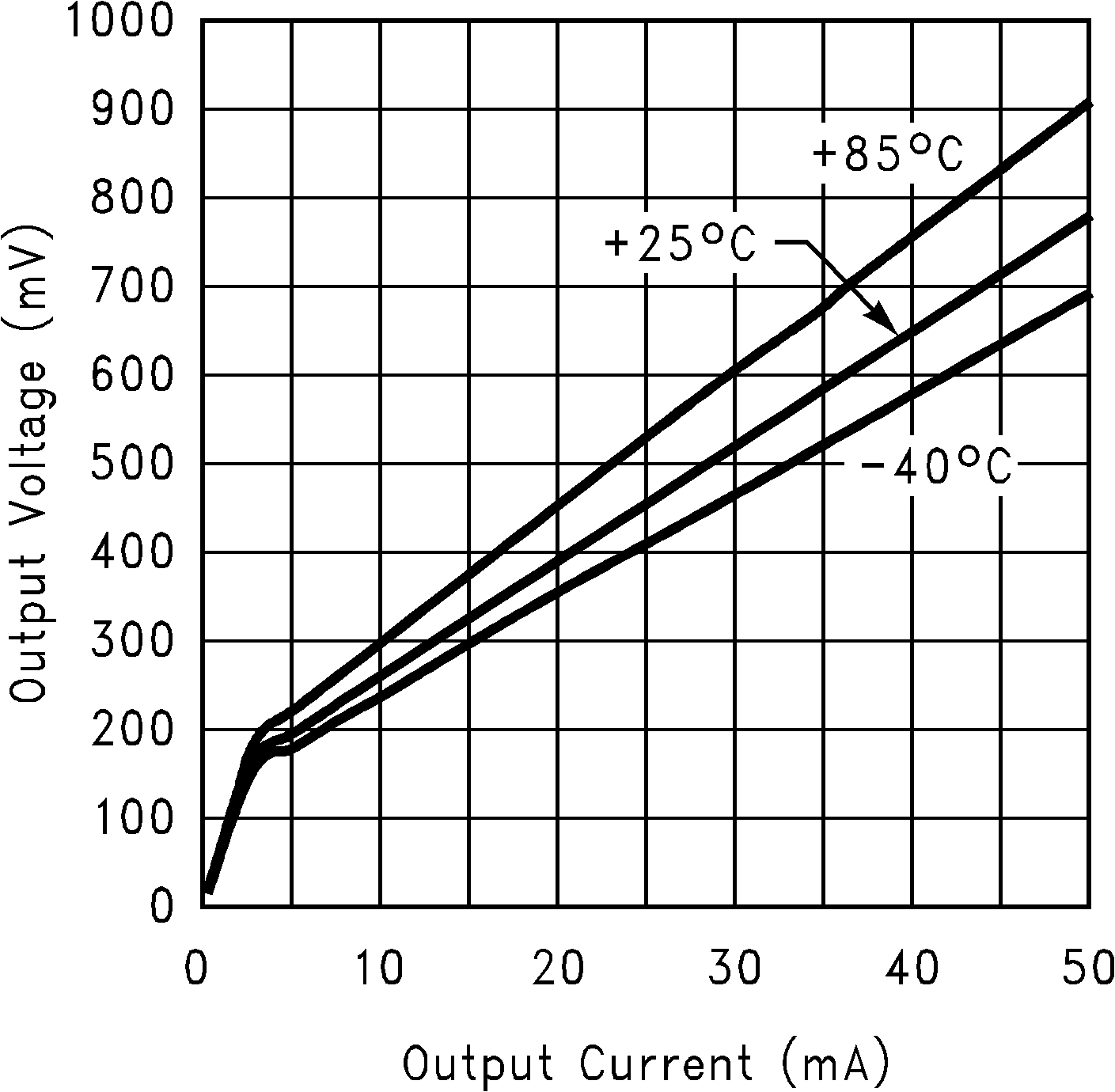
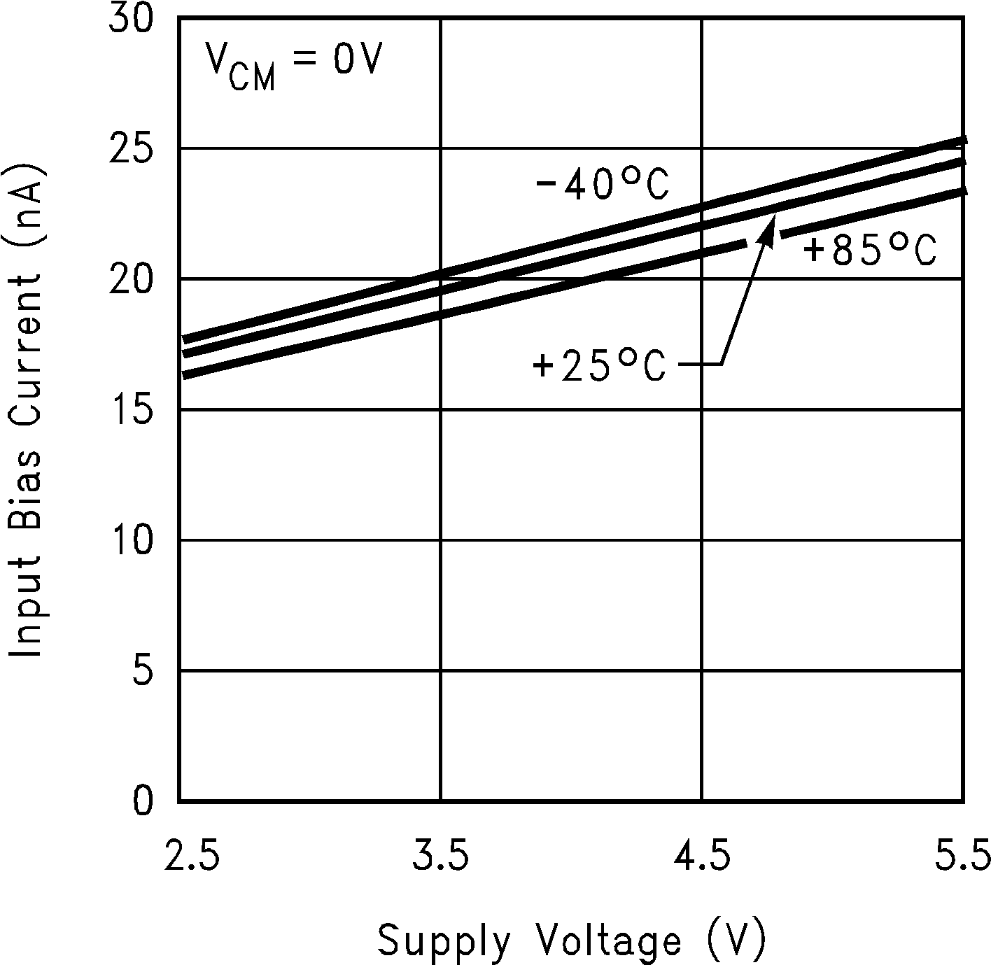
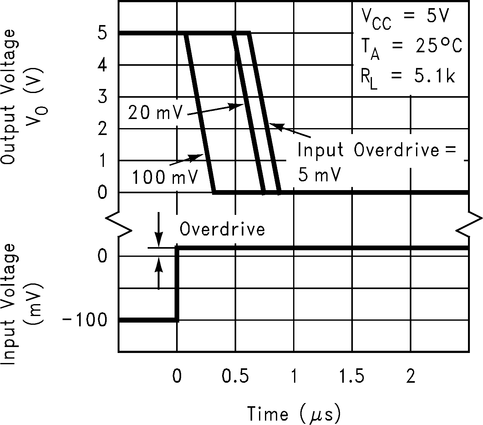
6.9 Typical Characteristics
Unless otherwise specified, VS = +5V, single supply, TA = 25°C